 Yann Guidon / YGDES
The series continues !
As I gain more insight into how this works, I can already shelf the previous design without trying it. Instead I gather and examine all the conditions and constraints of the design.
- The design must satisfy the Barkhausen criterion. My first attempts did not respect that, for example I forgot some passives (RC network) and the phase shift of the loop did not total 2π. The lousy transistors did not provide enough gain at the selected frequency.
- High selectivity (high Q factor): the intrinsic qualities of the crystal are affected by the surrounding parts. The less parts, the better. For example, less drift caused by heating components, less losses leading to better selectivity.
- Series or parallel mode : I still don't know the working mode of my tubes. I'll make a bet that it works but I can't be sure until my Rb clock is there.
- I want to add a visual indication that the tube is oscillating. More on this after the break.
- Gain control is very important ! Too much gain (or amplitude) is bad because it adds distorsions and harmonics, which de-tunes the circuit.
- (update 20160525:) The signal sent to the crystal must go somewhere. In the bipolar topologies, the base can act as a current sink but the isolated gates of MOSFETs acts as if the crystal was left unconnected on one end... More on this on another log.
Points 1) and 2) are addressed by the circuit with 2 cascaded BJT that works so well. I tried to make a MOSFET version but the gain was insane. Anyway, the cascade makes a 180µ180=360° phase shift and the crystal lets only the desired frequency pass through. Barkhausen is satisfied.
Part of my solution is to not use complementary pairs this time. MOSFETs provide a lot of gain so one of the MOSFET can have unity (negative) gain. The sense side would use a N-FET for example, and the drive side a P-FET, thus providing alternating bias levels and allowing a lower supply voltage.
The 2-transistors is also good because the gain is easy to set with adjustable resistors, there is only one capacitor to adjust. I have to find how to make the MOSFET's tempcos to cancel eachothers. The trimmers and the capacitor should be quite stable.
Point 4 is something else. It's not easy to visualise the oscillations without a 'scope so after I heard a lot "does this tube glow ?" I thought "ok I'll make it glow". Just shining a LED creates a cool effect, and the power can be derived from a single diode detector+capacitor. When the amplitude reaches a certain level, the extra power will go to the LED, showing that the ocillation is stable.
But wait, drawing current from the oscillator will affect it, in power, frequency and waveform/harmonics (the diodes have exponential characteristics). How can this be turned into an advantage ?
My approach is to turn the LED into an active part in the oscillator's loop, not only as an indication of signal level but also as a "soft peak limiter". So no diode-capacitor rectification. Direct clamping, à la Zener.
Diodes (and LEDs) have a negative tempco while MOSFET's tempco is positive so it might be a trick to compensate for temperature (if the tempcos are in the same order of magnitude). And since the LED has an exponential response, it doesn't affect the waveform too much.
If a red (or orange ?) LED is used, it will clamp/dampen the max sine amplitude to about 2V. This might also help regulate the circuit if the supply voltage fluctuates.
Biasing/polarisation of the two transistors is another story. If complementary types are used, they will not work at the same absolute voltage/level. A 10M resistor across them would help to bring them in the conduction zone.
OK, biasing with minimal parts count does not work. Forget the N and P-FET alternating idea.
The biasing kills everything, while the CMOS double-inverter circuit is naturally biased. The complementarity also helps compensate the tempco. The drawbacks are the gain control and the operation at low voltage.
But... Now I realise that I can reduce the gain very easily and without increasing the parts count ! It's just a matter of reducing/adjusting the biasing resistors' values !
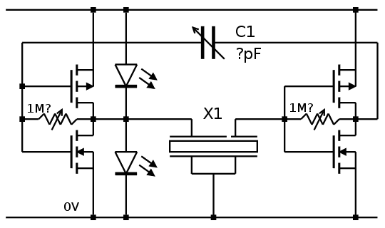
I added another LED to balance the signal and reduce harmonics.
This does not solve the problem of the higher supply voltage but it's something... I'll have to test it.
Could the left feedback resistor be replaced by a pair of parallel reversed diodes ? (thus adding some hysteresis) Germanium diodes have some leakage and can replace a resistor...
Update : The pair of diodes would be excellent replacements for the clamping LEDs ! Not only would they bias but also clamp/limit the amplitude in an even softer and power-efficient way. The clamping would be controlled by the forward voltage, so a pair of red LED indeed would limit the amplitude quite a bit.
Discussions
Become a Hackaday.io Member
Create an account to leave a comment. Already have an account? Log In.