 Michael O'Brien
Each display will be accompanied with 2 sets of LEDs: one for accent/backlighting, and the other for warning if a parameter gets [too] close or surpasses a use defined level. The catch with this was that I don't have various "control" lines to run over to each back of LEDs to turn one set on and another off and I'm using 3 colors on 2 PWM lines. Things became a bit tricky.
MOSFETs. And here I thought op amps were a pain... I quickly came to realize that I needed both an n-channel and a p-channel MOSFETs to act as normally open and normally closed switches. I could use the solid state relays I've come across, but those are $1-$1.50 a piece and 2 MOSFETs in 1 package of equivalent rating are less than 1/3rd to 1/2 the cost and have better thermals. Plus the SS relays have an switching times of about 10 ms where as the FETs are a few orders of magnitude faster.
The delay in creating the display boards is this circuit, though I've not explained what it does. My warning LED is a dual color, yellow and red, LED with a forward voltage of 1.95 and 2 v with a driving current of 20 mA. I don't need both on at the same time, but I only have 4 PWM lines. I've divvied them up to 1 line per display for the warning LEDs and the 4th line as general accent/backlight control. I ran across a problem in my theory of driving that dual-color LED: I could never have both turned off at the same time. This is even if I dial up the frequency and let the input/output capacitance of the FETs limit the on-off time as when that happens, the average voltage just climbs.
Well, I was ignoring one fact: I have the accent/backlight PWM line I can use. To minimize visual clutter, I'm in favor of turning off this light when a warning light comes on. Since those accent lights would be driven only part time, I would just need to use the on/off duty cycle to trigger to solid state relay. I was hoping to avoid using any of the SS relays, but hey, they are functional and a 10 ms delay before tuning one on isn't that big of a deal when I'm not rapidly changing its state. With that being said, I just needed to figure out some control circuits for driving the LEDs and below is what I came up with:
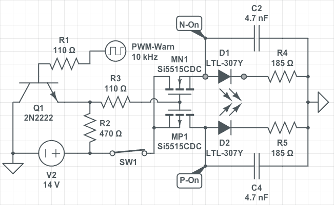
It's relatively simple circuit, modeled after the high-side load switch topology. The PWM signal rapidly turns Q1 on and off pulling the gates of the FETs to ground. R1 and R3 are current limiting. R2 is a pull down for the source of the N-channel FET so it can turn off, else it'd float on. If the value of R2 is increased above ~470 ohms, the capacitance of the FETs interfere with each other and alter duty cycle and on/off time of each other with a preference of keeping the p-channel FET on longer. I'd prefer a larger value, but I already have a limited 5-90% duty cycle due to roll off. R2 will have to be at least a 1W resistor. I updated the models with the info for the Si5515CDC dual FET from Vishay (pdf link). The caps, C2 and C4 are bypass caps to reduce the voltage spikes when the switch is open and the PWM signal is still active which is caused by overlap of the p-channel FET's slow turn off overlapping with the turn of the the n-channel FET. As they affect on-off time as well, I increased them to where their effect was minimal, but limited the transient spikes to about ~1.3V and ~-1.5V. SW1 will be replaced with the SS relay controlled via the accent/backlight off-time duty cycle, basically making it a low side switch so I don't have to worry about heat dissipation. The LED and current limiting resistor pairs are placeholder for the series/parallel/mixed LED arrays for the displays.
The highest draw LEDs that would be powered have a forward voltage of 4.9V, and a drive current of 20 mA. I'd need to drive 4 of them requiring 9.8V and 40 mA. I'll be using my 14V rail for juice and the Si5515CDC can give me at least ~55 mA @ 14V continuous at 50˚C, which is my internal maximum temperature threshold.
If my nomenclature is incorrect a couple paragraphs above, I blame it on not fully understanding the voltage relations of the source, drain, and gate on the FETs ;)
Discussions
Become a Hackaday.io Member
Create an account to leave a comment. Already have an account? Log In.