0%
0%
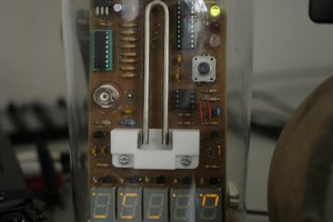
The "thIN-18" nixie tube clock
Simple and small 4-digit IN-18 clock.
 Gary Marsh
Become a Hackaday.io member
Already have an account? Log in.
Just one more thing
To make the experience fit your profile, pick a username and tell us what interests you.
Pick an awesome username
hackaday.io/
Your profile's URL: hackaday.io/username. Max 25 alphanumeric characters.
Pick a few interests
Projects that share your interests
People that share your interests


 Kris Slyka
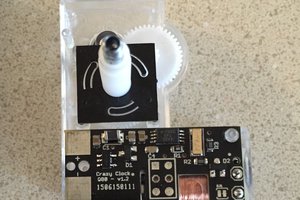
 Nick Sayer
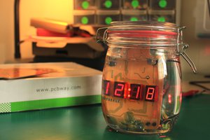
 Marius Taciuc
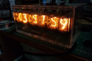
 sjm4306
i really love your design clean and simple. I have looked at the schematic, the power supply is a bit different than other supplies used in nixie clocks can you give me some more details about it ? :)