-
HyTech Battery Management System Segment
10/29/2021 at 17:06 • 0 commentsHyTech Racing is an award-winning student-run organization at the Georgia Institute of Technology dedicated to furthering students' engineering experience through the rigorous design and development of Formula SAE electric vehicles. Every year, we design, build, and race a brand new student-designed single seater electric formula style racecar. Thanks to JLCPCB for providing us with this sponsored PCB.
HyTech Battery Management System (BMS) Segment
![]()
HyTech Racing utilizes a custom battery pack with a nominal voltage of 310V that is split into four battery segments of 21 cells each. Each battery segment is monitored by its own BMS segment, resulting in a semi-distributed battery management system.
![]()
The 21 cells are connected to the BMS segment through the use of spring contacts that are soldered to the pads shown above. This allows the BMS segment to maintain electrical contact with the batteries under the vibrations and shocks the pack experiences while the vehicle is in motion.
![LTC6811 12-Channel Multi-Cell Battery Monitor - ADI | Mouser]()
At the heart of the battery management system segment are two LTC6811-2 multicell battery monitors from Analog Devices. This IC can monitor the voltages of up to 12 cells in series, taking voltage readings with total measurement error of less than 1.2mV at a user-selectable data acquisition rate. Each of HyTech's battery segments contains 21 cells, which results in an architecture where one IC monitors 9 cells, while a second monitors 12 cells. Each chip is independently addressable, with the chip addresses set through the use of jumper resistors to represent the address in binary. The IC communicates through isoSPI, a proprietary version of the SPI protocol that uses a twisted pair to achieve isolation and allows us to read data on our control unit.
![NTC Thermistor, THT, 10K, Tmin: -40°C, Tmax: 150°C NTC 640-10K | GM electronic COM]() Battery temperatures are monitored using thermistors that in contact with metal directly touching the battery leads. Using the GPIO available on the LTC6811, temperature data is transferred to the control unit, allowing HyTech to monitor for safe temperatures. The LTC6811 also internally monitors IC temperature, and the board also contains two dedicated temperature and humidity sensors to monitor for ambient temperature and water ingress inside the battery pack container.
Battery temperatures are monitored using thermistors that in contact with metal directly touching the battery leads. Using the GPIO available on the LTC6811, temperature data is transferred to the control unit, allowing HyTech to monitor for safe temperatures. The LTC6811 also internally monitors IC temperature, and the board also contains two dedicated temperature and humidity sensors to monitor for ambient temperature and water ingress inside the battery pack container. PCB Fabrication at JLCPCB
The BMS Segment PCB fabrication has been generously sponsored by JLCPCB. Their quick turnaround times and high quality products allow us to prototype our designs more efficiently and effectively. Ordering from JLCPCB is simple: simply hit the Order Now button, upload your gerber zip file, and you're all set! HyTech frequently uses and highly recommends JLCPCB for PCB fabrication needs.
-
HyTech Sensor Acquisition Board
06/26/2021 at 00:18 • 0 commentsHyTech Racing is an award-winning student-run organization at the Georgia Institute of Technology dedicated to furthering students' engineering experience through the rigorous design and development of Formula Student electric vehicles. Every year, we design, build, and race a brand new student-designed single seater electric formula style racecar. Thanks to JLCPCB for providing us with this sponsored PCB.
I. Introduction
Data acquisition is an important portion of the HyTech team that focuses mainly on optimization. They do this by continually taking in inputs from the car. Some of these inputs are external, such as speed or temperature, while others are internal, such as battery levels. Without taking these parameters into account, it would be significantly harder to perform optimizations. To help out, the low voltage team was tasked with creating a board that can collect the data for the sensors, which resulted in the Sensor Acquisition Board.
II. Data Input
Figure 1. This is one of the sensor inputs that shows the connector, OpAmp, and filter Each sensor is connected to the board via a Molex connector that carries power, ground, and the signal. The signal is then fed directly into an operational amplifier (OpAmp) to strengthen the signal so it can be read and interpreted better. Directly from the OpAmp, the signal goes into a MAX7400 IC, whose job is to filter. Filtering removes a lot of external noise that might show up as false data and mess with any analysis and provides for a better overall signal.
III. ADC
Figure 2. The MCP3204 and its inputs are shown. Once cleaned up, the signal is sent to the MCP3204 IC, which is an analog to digital converter (ADC). This is necessary because while most things in the real world have analog values (ie. values in a continuous range), computers speak in the language of 1s and 0s. The ADC is responsible for taking these digital values and converting them into a string of 1s and 0s that can be interpreted by a microcontroller.
IV. CAN Communication and Microcontroller
Figure 3. The microcontroller and CAN terminals interfacing are shown. Finally, the data can now be sent to a microcontroller. Using the serial port interface (SPI), the microcontroller can be told which input it needs to look at. CAN allows for these microcontroller signals to be sent along to the MCP3204, telling it what to transmit. CAN allows for easy signaling and has the advantages of built-in error detection and speed.
V. Final Steps
Once we finished designing our board, we got them manufactured at JLCPCB. To manufacture your own PCBs, you can use JLCPCB at https://jlcpcb.com/RAT. Just hit “QUOTE NOW” to order your custom PCB. Our team chooses JLCPCB because of the high quality for the price and timely manufacturing.
-
HyTech Charger Controller Design
03/04/2021 at 03:03 • 0 comments![]()
HyTech Racing is an award-winning student-run organization at the Georgia Institute of Technology dedicated to furthering students' engineering experience through the rigorous design and development of Formula Student electric vehicles. Every year, we design, build, and race a brand new student-designed single seater electric formula style racecar. Thanks to JLCPCB for providing us with this sponsored PCB.
I. Introduction
![]()
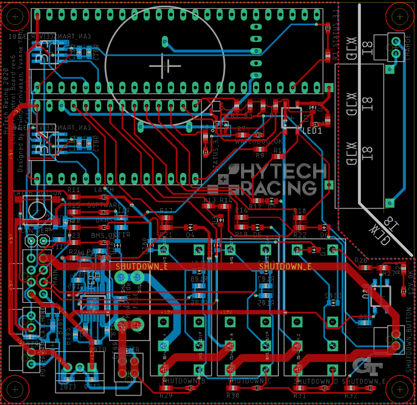
The charger controller board is used in our electric formula-style racecar to manage our battery pack's charging in a safe, efficient way. This custom designed board has many features, focusing on both safety and data collection. The brains of the board lies in two microcontrollers, a Teensy 3.2 for the main controlling of the charger and safety features and a Teensy 3.5 for data logging.
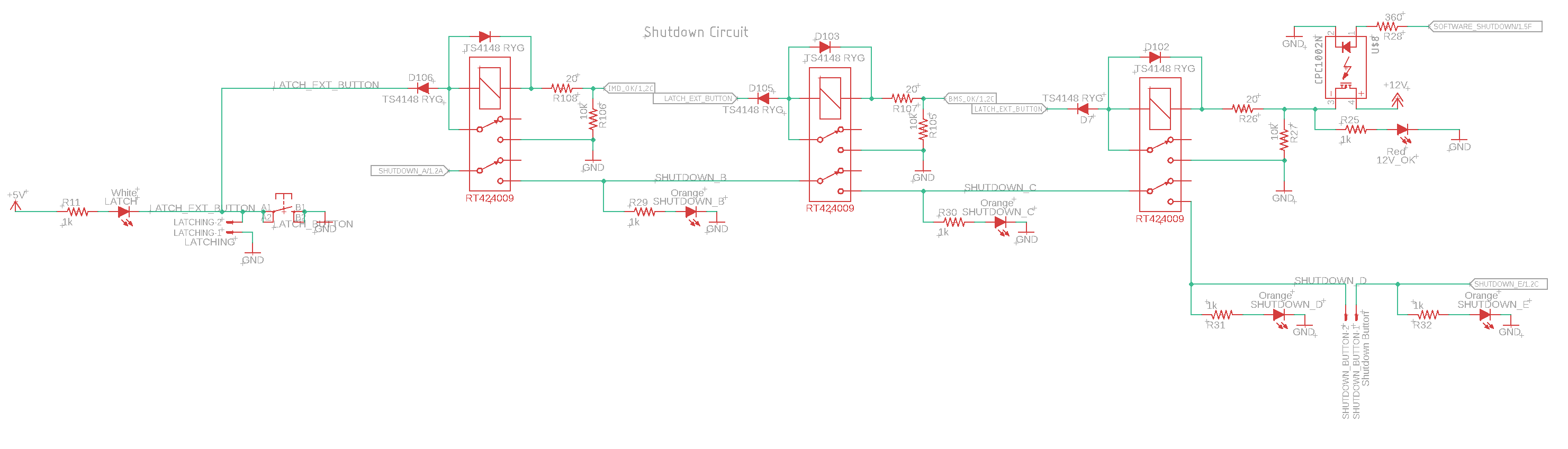
II. Shutdown Circuit
![]()
Figure 1. Schematic of the shutdown circuit including the relays and latching circuitry.
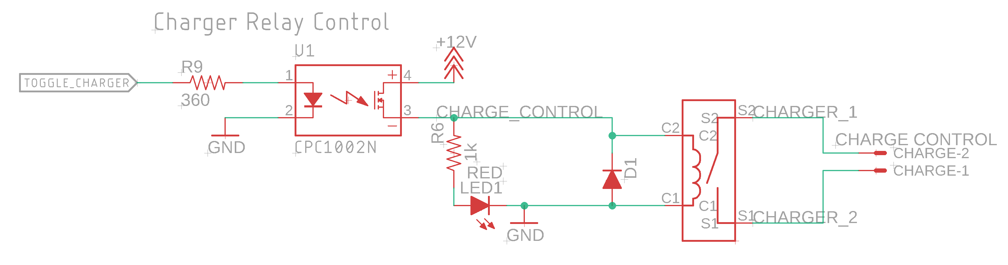
The shutdown circuit is the main safety feature of the board, consisting of three stages. Each stage must be active (driven high) in order for charging to commence. Each of these three signals also contain a latching circuit to ensure once a fault happens, the charger remains off until the issue is resolved and the system is reset. An isolated relay is used to control the charger control signal to prevent damage if a fault in the charger occurs.
![]()
Figure 2. Schematic showing the isolated control signal between the shutdown circuit and the chargers toggle.
Car's Shutdown Signals
Onboard the car, there are many additional fault systems in place, including a signal that provides the status of the battery management system (BMS) and another signal providing the status of the insulation monitoring device (IMD). These two signals, the IMD_OK and BMS_OK, are directly connected to individual relays in the shutdown circuit on the board. If either of these signals are low, the shutdown circuit will immediately trip, stopping the charge until the issue is resolved and the system is reset.
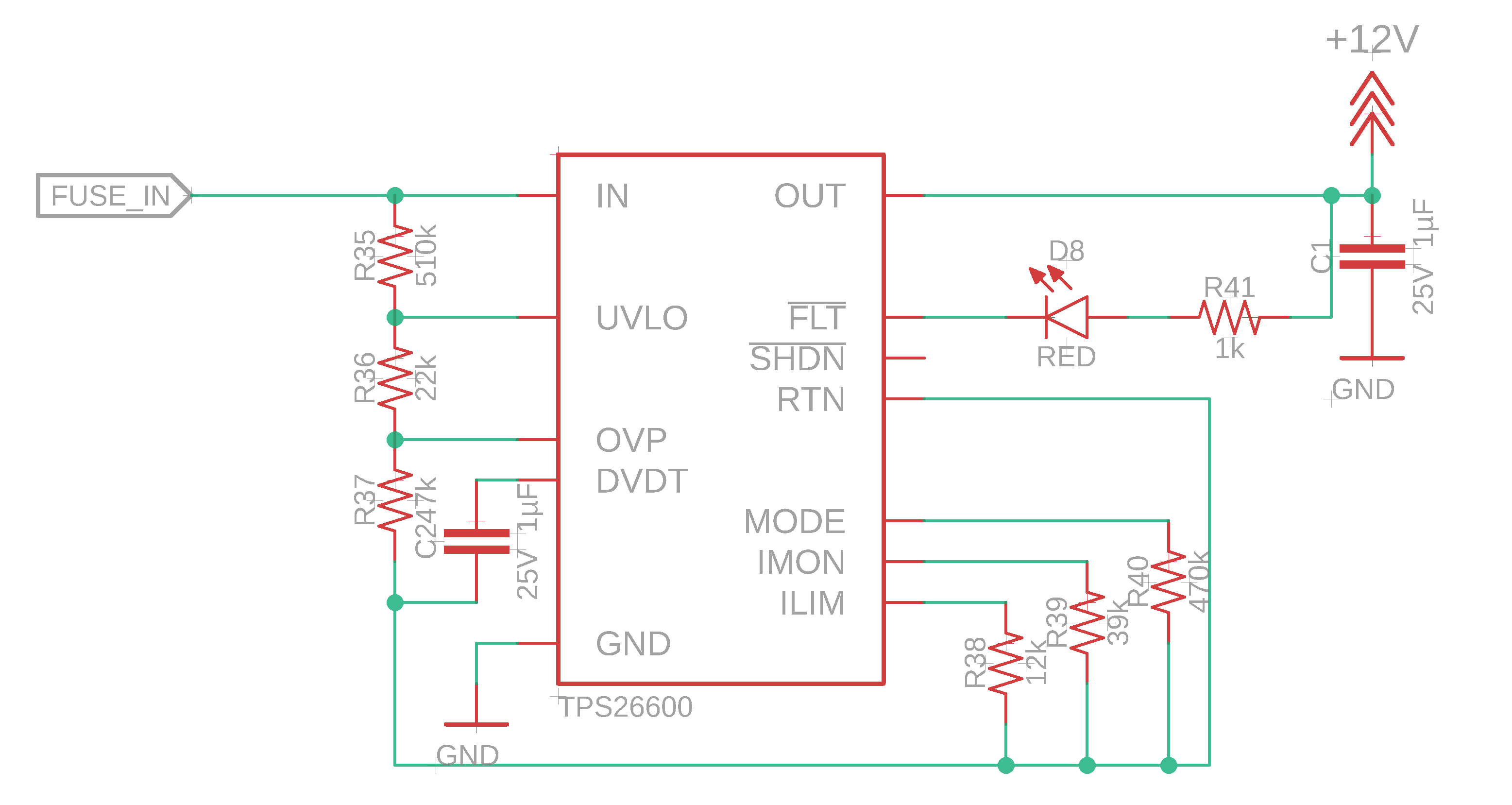
E-Fuse
![]()
Figure 3. Schematic showing the implementation of the e-fuse into the board.
The E-fuse is the second safety mechanism, monitoring the current flowing and providing information to the onboard Teensy 3.2. The Teensy can then deem the current to be a fault state (too high, abnormal, etc.) and shutdown the charger with the final relay in the shutdown stage. This current value is also displayed to the serial connection of the Teensy 3.2 for charge progress and monitoring.
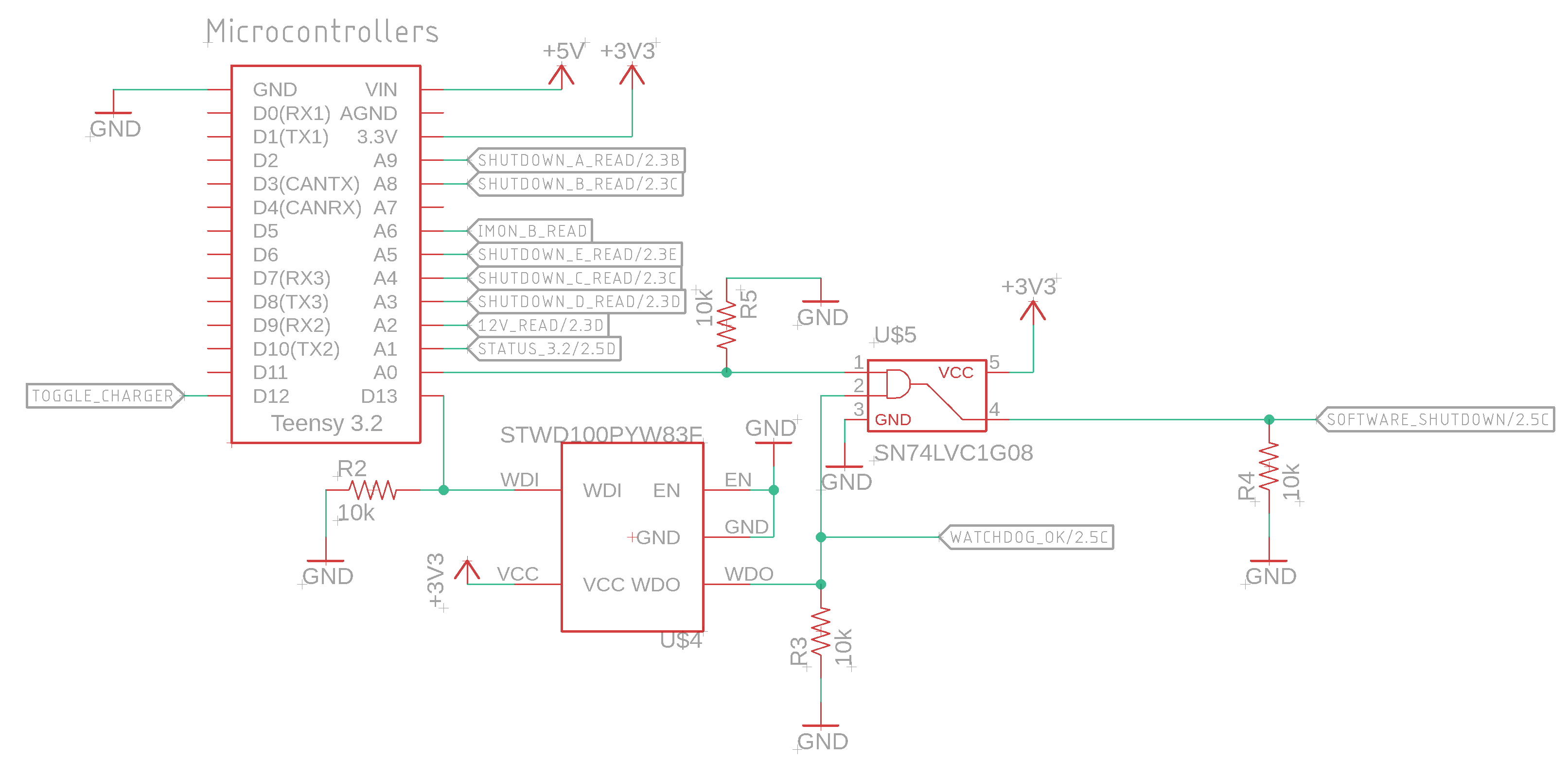
Watchdog Timer
![]()
Figure 4. Schematic showing the watchdog circuit in place to catch microcontroller faults.
The final safety mechanism incorporated on this board is a watchdog timer to ensure the Teensy 3.2 is operating properly. The watchdog timer requires a signal from the Teensy and if that signal is not received, the watchdog timer will trip the shutdown circuit, once again turning off the charger. This system is in place to catch anytime the Teensy freezes, stops, or crashes to ensure a safe shutdown of the charger.
The board has been designed with many redundancies to ensure charging occurs safely and consistently. If one system fails, another system will always catch that failure before any damage or safety is compromised. This allows our team to be efficient yet confident while charging our car's battery pack.
III. Final Steps
![]()
Once we finished designing our board, we had to get them manufactured. To manufacture your own PCBs, you can use JLCPCB, at https://jlcpcb.com/RAT. Just hit “QUOTE NOW” to order your custom PCB. Our team chooses JLCPCB because of the high quality for the price along with timely manufacturing.
![]()
Figure 5. Charger Controller PCB arrived in shop after manufacturing by JLCPCB.
My Pages


 Battery temperatures are monitored using thermistors that in contact with metal directly touching the battery leads. Using the GPIO available on the LTC6811, temperature data is transferred to the control unit, allowing HyTech to monitor for safe temperatures. The LTC6811 also internally monitors IC temperature, and the board also contains two dedicated temperature and humidity sensors to monitor for ambient temperature and water ingress inside the battery pack container.


 Once we finished designing our board, we got them manufactured at JLCPCB. To manufacture your own PCBs, you can use JLCPCB at

Share this profile
ShareBits
Become a Hackaday.io Member
Create an account to leave a comment. Already have an account? Log In.