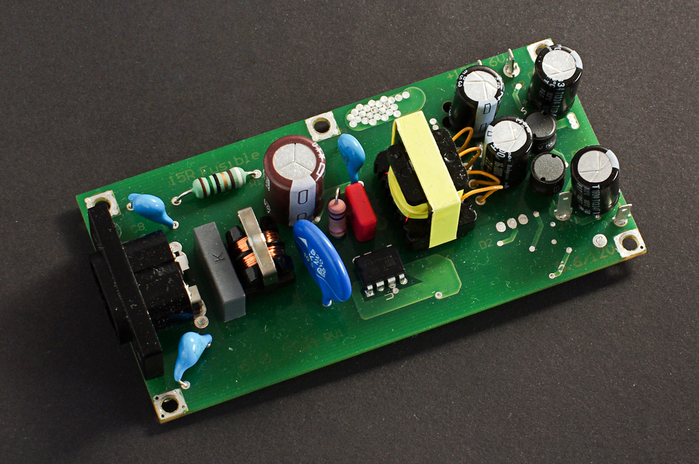
In the realm of printed circuit board (PCB) design, electromagnetic interference (EMI) and electromagnetic compatibility (EMC) are crucial concepts that influence the performance and reliability of electronic devices. This article aims to provide an overview of EMI and EMC, explaining their significance in PCB design and the measures taken to mitigate their effects. Understanding EMI and EMC is essential for engineers to ensure that electronic systems function optimally and comply with electromagnetic compatibility standards.

Electromagnetic Interference (EMI)
Electromagnetic interference (EMI) refers to the unwanted electromagnetic emissions or disturbances that can disrupt the normal operation of electronic devices. EMI can arise from various sources, such as electromagnetic radiation from nearby devices, power supply fluctuations, switching components, or external electromagnetic fields. These interference sources can induce noise, voltage spikes, or signal distortions, leading to signal integrity issues and malfunctions in the affected circuitry.
To mitigate EMI, PCB designers employ several techniques. Proper grounding and shielding techniques are crucial to minimize electromagnetic emissions and susceptibility. Careful routing of high-speed signal traces and power planes, as well as the strategic placement of decoupling capacitors, can also help reduce EMI effects. Additionally, using EMI filters, ferrite beads, and shielding enclosures are effective measures to suppress electromagnetic interference.
Electromagnetic Compatibility (EMC)
Electromagnetic compatibility (EMC) is the ability of an electronic system to function properly in its intended electromagnetic environment without causing interference to other devices. Achieving EMC involves both controlling the emissions of a device (EMI) and ensuring its immunity to external electromagnetic disturbances.
PCB designers employ various EMC design practices to achieve compliance with EMC standards. This includes designing PCB layouts that minimize loop areas and provide proper impedance control. Ground and power planes should be carefully designed to reduce common mode and differential mode noise. The use of proper bypass capacitors and filtering techniques can help maintain clean power supplies and mitigate conducted emissions.
EMC Testing and Compliance
EMC testing is a critical phase in PCB design to verify the device's electromagnetic compatibility. Compliance with EMC standards is essential to ensure reliable operation and avoid potential issues caused by interference. EMC testing involves assessing the emissions and immunity of the device under specific test conditions.
Emissions testing evaluates the radiated and conducted emissions from the device, ensuring they are within acceptable limits. Immunity testing, on the other hand, determines the device's ability to withstand electromagnetic disturbances without malfunctions. Common EMC tests include radiated emissions testing, conducted emissions testing, electrostatic discharge (ESD) testing, and electromagnetic field immunity testing.
Conclusion
EMI and EMC are critical considerations in PCB design to ensure the reliable and efficient operation of electronic devices. By implementing proper design techniques and employing effective EMI/EMC mitigation measures, PCB designers can minimize the risks of interference and non-compliance with electromagnetic compatibility standards. A thorough understanding of EMI and EMC allows engineers to create robust PCB layouts and electronic systems that can function optimally in their intended environments while maintaining compliance with industry standards.
Related Articles:
 Sam
Sam
Discussions
Become a Hackaday.io Member
Create an account to leave a comment. Already have an account? Log In.