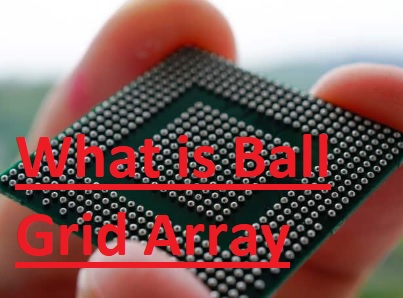
Hi, guys welcome to the new post. In this post, we will discuss What is Ball Grid Array (BGA) on a PCB Board. Ball Grid Array (BGA) is a packaging technology commonly used in electronic circuit boards that have different advantages than other traditional packaging techniques. It is popular due to its ability to accommodate larger interconnections in a small area, so it is best for high-density applications. In this post, we will learn Ball Grid Array (BGA), and other parameters. So let's get started What is Ball Grid Array (BGA)
What is BGA?
- BGA is a surface-mount packaging type where solder balls are configured in a grid-like pattern on the bottom of a component. These solder balls create electrical connections between components and the PCB board. BGA packages are the main part of microprocessors, integrated circuits, and other complicated electronic components.
[adinserter block="3"]
BGA vs. Other Packaging Technologies:
| Feature | BGA | PGA | LGA |
|---|---|---|---|
| Package type | Ball grid array | Pin grid array | Land grid array |
| IC connection | Solder balls | Pins | Solder balls |
| Package size | Compact | Larger | Larger |
| Heat dissipation | Good | Fair | Good |
| Cost | expensive | Less costly | Less costly |
| Complexity | More complicated | Less complicated | Less complicated |
| Applications | High-performance devices, devices with a lot of ICs thin devices, | General-purpose devices, devices that do not need high performance | General-purpose devices, devices that do not need high performance |
Advantages of BGA:
BGA has different advantages that make it the best for different PCB designs. Firstly, the small size package size allows for more components to be connected on the PCB, leading to higher functionality in a small area. 2nd, the shorter electrical paths between the component and the board improve signal integrity. BGA's thermal features also enable efficient heat dissipation, so they are good for high-power applications.
BGA Assembly Process:
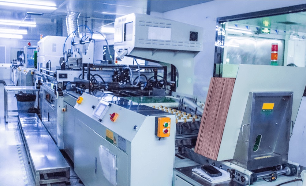
The BGA assembly has different steps. It started with the application of solder paste on the board, followed by component placement with the use of automated machines. The PCB board then passes reflow soldering, where the solder balls melt and make reliable electrical connections. After cooling, the PCB board undergoes inspection to make sure proper alignment and solder joint quality.
Challenges in BGA Assembly:
BGA assembly also has unique challenges. The Main is the accurate alignment of the BGA component due to the absence of leads. BGA components also needed accurate control of the reflow soldering process to avoid problems like solder bridging and voids. With that, the inspection of hidden solder joints and the detection of defects pose additional problems
BGA Inspection and Testing:
Various inspection and testing techniques are employed to make sure the quality and reliability of BGA components. X-ray inspection is used to find hidden solder joints, while optical inspection systems can find defects on the component surface. With that, electrical testing, like ball shear, and ball pull tests, are done to assess the mechanical strength of the solder joints.
BGA Rework and Repair:
For faulty BGA components, rework and repair methods are employed. BGA rework does removing the defective component, cleaning the site, and replacing them with new ones. This process needs advanced tools and skilled operators to avoid damage to the board and adjacent components.
[adinserter block="5"]
BGA Reliability:
BGA packages provide high reliability due to their robust electrical and thermal connections. Though, some factors like mechanical stress temperature cycling, , and aging can affect their long-term performance. Accurate design considerations, material selection, and assembly methods are used to ensure the reliability of BGA components.
Types of BGA
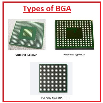
1. Ceramic BGA (CBGA):
Ceramic BGA packages are made with the use of ceramic materials and offer excellent thermal properties and high reliability. The ceramic substrate has good heat dissipation, making CBGA the best for applications that produce significant heat. CBGA packages are famous for their durability, making them best in harsh environments and high-performance electronic devices.
2. Plastic BGA (PBGA):
Plastic BGA packages use plastic as the base material. They are cost-effective solutions for different electronic applications. These packages come with a plastic substrate that has insulation and mechanical support. They are used in consumer electronics, like smartphones, laptops, and gaming consoles, where cost and space considerations are significant.
3. Flip Chip BGA (FCBGA):
Flip Chip BGA packages are made for high-density applications and provide good electrical performance. In FCBGA, the IC is flipped upside down and mounted onto the substrate, making shorter interconnects and reducing signal delay. This design has lower power consumption higher frequencies,, and improved thermal characteristics.
4. Micro BGA (MBGA):
Micro BGA packages are compact types of BGA and have a smaller footprint and pitch. They are used in space-constrained applications, like mobile devices, where miniaturization is important. MBGA packages have high-density interconnections and are made to accommodate the ever-shrinking size requirements of modern electronic devices.
JLCPCB BGA Technology:
As a well-known and reputable supplier of PCB manufacturing and assembly services, JLCPCB includes BGA manufacture as a significant component of their vast range of services. The BGA (Ball Grid Array) technology is only one of the many technologies and functions they provide. Their area of competence is the production and assembly of PCBs with BGA packages. A grid of solder balls makes up BGA packages, which are renowned for their cutting-edge packaging technique and enable high-density interconnections. The BGA-PCB products are tested and examined by JLCPCB using a very effective technique before being finished and sent to clients.
The BGA manufacturing services provided by JLCPCB are specially designed to meet the requirements of modern electronics, guaranteeing that the various needs of clients for BGA integration into their PCB designs are satisfied to the highest degree of accuracy and quality.
. They are able to manage BGA packets of various shapes and dimensions. Here are some of their BGA technology's salient features:
- Advanced Manufacturing Equipment: JLCPCB uses cutting-edge production tools, like reflow ovens and precision placement machines, to make sure the accurate and dependable placement of BGA components on board.
- High-Precision Assembly: BGA components require accurate alignment and soldering methods to ensure optimal electrical connections. JLCPCB uses advanced assembly processes and methods to get high-quality BGA soldering.
- X-ray Inspection: Visual examination of BGA solder junctions is difficult since they are frequently concealed behind the packaging. JLCPCB uses X-ray inspection tools to monitor the alignment and soldering integrity of BGA solder connections.
- Design Guidelines: For PCBs containing BGA components, they offer design recommendations to assist clients in maximizing their designs for successful production and assembly. These recommendations frequently address topics like solder mask clearance, pad design, and thermal considerations.
- Quality Assurance: Strict quality control procedures are used by JLCPCB to make sure the dependability and performance of BGA assemblies. To check the functionality of BGA components, they could conduct a range of tests, including electrical and functional testing.
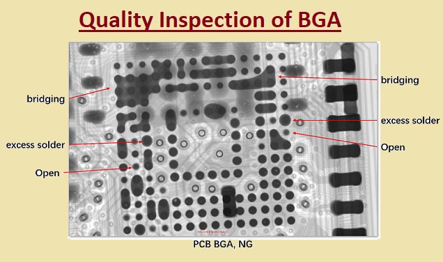
Quality inspection of BGA
Quality inspection of BGAs is significant to make sure that the solder joints are accurately formed and that the IC is mounted correctly on the PCB. There are a number of different techniques that can be used to inspect BGAs, including:
[adinserter block="6"]
- Visual inspection: This is the basic method of inspection and performs visual checking of the solder joints for any defects, like cracks, voids, or cold solder joints.
- Automated optical inspection (AOI): it is an advanced method of inspection that uses a computer to automatically scan the BGA faults. AOI systems can detect a different range of defects than visual inspection.
- X-ray inspection: it is an accurate process of inspection and can be used to detect even the smallest faults in the solder joints. X-ray inspection is used in high-reliability applications, like military and aerospace.
Defects of BGA
- Cold solder joints: This produces when the solder does not correctly wet the surface of the IC or the board. This can cause poor electrical connections and can eventually result in the failure of the IC.
- Voids: Tit causes when there are air pockets in the solder joint. This can make poor electrical connections and can eventually lead to the failure of the circuits.
- Cracks: It happens when the solder joint is not strong enough to withstand the stresses that are applied to it.
Elimination of BGA defects:
Detaching of components: BGA component defects can be rectified by first detaching the components from the board. It can be done by careful heating of localized components on the PCB board, which melt down the solder joints, and we can vary the components and fix the solder connections as needed
BGA rework process: This process is done in a dedicated rework station in the factory., where BGA board components are heated with the use of the infrared heater. Heat level can be monitored by thermocouple. To raise the package from the underlying board a vacuum module is used along with other equipment.
Localized heating: the heating method is done carefully and it is limited to the defective area on the PCB board. Localized heating to confirm the safety of neighboring components on the PCB.
FAQs
What is a BGA in PCB?
A BGA, or ball grid array, is surface-mount packaging used for integrated circuits. BGA packages are employed to permanently mount devices, graphics processing units (GPUs), microprocessors, and memory chips. BGA packages are more compact than traditional pin-grid array (PGA) packages, and they allow for better heat dissipation.
[adinserter block="6"]
What is the difference between BGA and LGA?
BGA and LGA are types of surface-mount packaging. The difference between them is that solder balls on BGA packages are located on the IC circuit's bottom, whereas solder balls on LGA packages are located on the IC's top. Because of this difference in design, BGA packages are smaller than LGA packages, but LGA packages are simpler to solder.
What is the difference between a pin grid array and a ball grid array?
The basic difference between pin grid array (PGA) and ball grid array packages is the way that the IC is attached to the baord. In a PGA package, the IC has pins that fit into holes on the board. In BGA packaging, the IC has solder balls that are connected on a grid pattern on the board. The solder balls melt in the soldering process, creating a connection between the IC and the board
What is the difference between PCB and BGA?
A PCB,, is a board that has conductive pathways that allow electrical components to be attached together. A ball grid array, is a type of IC packaging that uses solder balls to connect the IC components to the PCB.
What are the 3 types of PCB?.
- Single-sided PCBs have conductive pathways on one side of the
- Double-sided PCBs have conductive pathways on both sides of the board.
- Multilayer PCBs have conductive pathways on multiple layers of the board.
What is the function of BGA?
The function of a BGA is to connect an IC to a PCB. The solder balls on the bottom of the BGA melt during the soldering process, making the connection between the IC and the PCB.
What is the advantage of BGA?
BGA packaging has different advantages than traditional PGA packages. BGA packages are compact and used for smaller devices. These packages also allow for good heat dissipation, that is important for devices that generate a lot of heat.
How many types of BGA are there?
There are many different types of BGA packages, Some are listed here
- Low-profile BGA packages are designed for use in thin devices.
- High-density BGA packages are designed for use in devices with a lot of ICs.
- Flip-chip BGA packages are designed for use in devices that require high performance
Discussions
Become a Hackaday.io Member
Create an account to leave a comment. Already have an account? Log In.