-
Overview of Flex PCB Panels: Definition, advantages, and applications.
06/22/2023 at 11:20 • 0 commentsHello friends welcome to the new post. In this post, we will discuss the Overview of Flex PCB Panels: Definition, advantages, and applications. Flex PCB panels have revolutionized the world of printed circuit boards by providing a flexible and versatile alternative to rigid boards. With their ability to twist, bend, and conform to different shapes, flex PCB panels are essential components in different industries. In this post, we will discuss the definition, advantages, and use of flex PCB panels, also design considerations
Introduction to Flex PCB Panel
[adinserter block="3"]
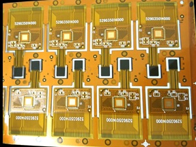
The continuous development of electronic devices and the need for smaller, less-weight, and more compact designs are lead to the creation of flex PCB panels. These panels are created with flexible materials that allow for three-dimensional flexibility, making them best for applications where space constraints and complicated form factors exist. With their flexibility, flex PCB panels provide different advantages to rigid PCBs, making them the best for different industries.
![flex pcb pannels]()
What is a Flex PCB Panel?
A flex PCB panel, also called a flexible printed circuit board, is a PCB board that is constructed with the use of flexible substrate materials, like polyimide or polyester films. These materials offer the required flexibility, and help PCB to be twisted, bent, or folded without compromising its electrical integrity. The flex PCB panel has conductive traces and pads that interconnect electronic components mounted on the board.
Advantages of Flex PCB Panels
Flexibility and Bendability
One of the main advantages of flex PCB panels is their flexibility and bendability features. Unlike rigid boards, which are fixed in structure, these panels can be flexed or bent to fit into tight spaces or conform to complicated form factors. This flexibility is used for more compact and innovative product designs, especially in projects where space is limited.
Space-saving Design
Flex PCB panels enable space-saving designs by eliminating the need for bulky connectors and cables. The flexibility of the PCB itself allows for the direct routing of traces, minimizing the need for additional wiring. This reduction in space requirements can be particularly beneficial in portable electronic devices, where size and weight are critical factors.
Enhanced Durability
They are highly durable due to their flexible manufacturing. Contrary to rigid PCBs, which can be prone to mechanical stress and failures in high-vibration environments, these panels can withstand twisting, bending, and repetitive motion without compromising their functionality. This durability makes them best for applications that needed reliable function under harsh conditions.
Improved Signal Integrity
The flexibility of panels decreases the occurrence of signal interference and impedance mismatches. By allowing traces to be routed directly, the length and complications of signal paths can be reduced, it enhances signal integrity. This benefit is significant for high-frequency and high-speed applications, where signal quality is needed
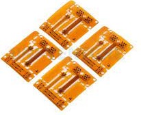
Cost-effectiveness
While the initial cost of panels can be larger than that of traditional rigid boards, they can provide cost savings in the long run. The reduction of connectors and cables, also reducing the need for additional assembly steps, can cause in lower material and labor expenses. Though, the compact size and less-weight nature of flex panels can lead to savings in shipping and handling costs.
![flex pcb panels]()
Applications of Flex PCB Panels:
[adinserter block="5"]
Consumer Electronics
In consumer electronics, like tablets, smartphones, wearables, and portable gaming devices, flex panels are used to accommodate the slim and compact designs required by consumers. They are used for the seamless integration of electronic components, like displays, touch sensors, and batteries, in space-constrained modules
Automotive Industry
The automotive industry uses these panels...
Read more » -
What are the Steps Flexible PCB Manufacturing Process
06/20/2023 at 12:23 • 0 commentsHello readers welcome to the new post. In this post, we will learn What are the Steps Flexible PCB Manufacturing Process. Flexible Printed Circuit Boards are very popular due to their features to provide good flexibility and reliability in different electronic applications. They provide many advantages over rigid PCBs, like enhanced space utilization, good reliability, and increased design flexibility. In this post, we will learn different factors for the flexible PCB manufacturing process. So let's get started with Flexible PCB Manufacturing Process
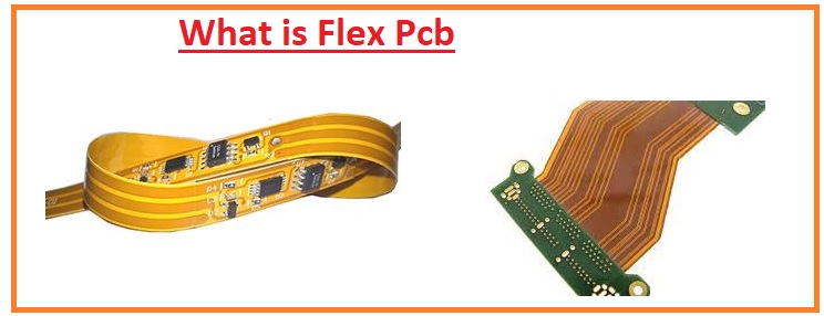
Introduction to Flex PCB
Flexible PCBs, also called flex circuits or flex boards, are electronic interconnects that can twist, bend, and fold without having an effect on their functionality. They have a thin, flexible substrate created by polyimide or polyester, which helps them to conform to complicated structures and fit into tight spaces. Flex circuit manufacturing comes with different steps, ensuring the manufacturing of high-quality, reliable boards.
[adinserter block="3"]
Understanding Flexible PCBs
Before going to discuss flexible pcb manufacturing, let's discuss the fundamental parameters of flexible PCBs. These circuit boards have 3 main layers: the substrate, conductive traces, and protective cover layers. The substrate work as the base and offers flexibility, while the conductive traces, created with copper, establish electrical connections between components. The protective cover layers protect the traces and make sure durability.
Benefits of Flexible PCBs
Flexible boards provide many advantages that make them best for various industries. Firstly, their flexibility is used for seamless integration into compact and irregularly shaped devices, optimizing space use. 2nd, their less-weight nature decreases the total weight of the electronic assembly. Also, the absence of connectors and the ability to remove complicated wiring harnesses make simple the assembly process, decreasing manufacturing time and costs. Though, the flexibility of these circuits decreases the chances of mechanical failures due to vibrations or shock, and improves overall reliability.
![what is flx pcb]()
Designing a Flexible PCB
Designing a flexible board needed careful consideration of the application's needs, mechanical constraints, and electrical features. It is necessary to select the accurate substrate material, find the number of layers, and define the circuit's layout. The design process consists of optimizing the placement of components, routing traces, and making sure of proper signal integrity. Advanced design software and professional skills in flex circuit design are important to get optimal results.
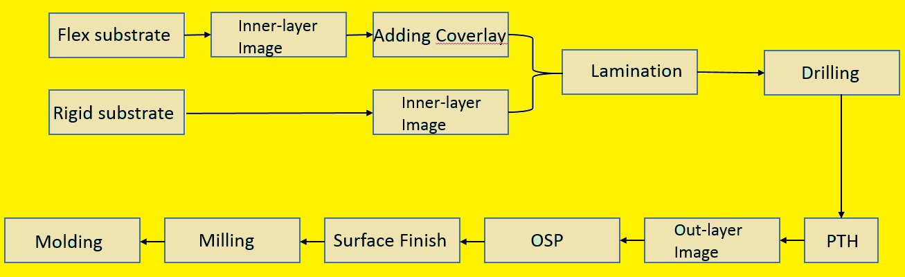
Steps in the Flexible Printed Circuit Manufacturing Process
![Flexible Printed Circuit Manufacturing Process]()
Step 1: Material Selection
The first step in flexible printed circuit manufacturing is selecting accurate materials. The selection of substrate material is based on parameters like thermal stability, flexibility, dielectric properties, and cost. Polyimide and polyester are commonly used due to their high-temperature resistance, excellent flexibility, and electrical insulation features. The conductive traces are made of copper due to its good electrical conductivity.
Step 2: Circuit Design
After the selection of materials, the next step is circuit design. That makes a schematic diagram of the circuitry, explaining the component placement and determining the routing of traces. The circuit design makes sure optimal electrical performance, signal integrity, and adherence to design rules.
Step 3: PCB Layout
In this step, the circuit design is converted into a physical layout. The layout consisting placing components on the flexible substrate and routing the traces to make electrical connections. Attention to detail is important to confirm the accurate alignment of components and reduces signal interference.
Step 4: PCB Printing
After the layout is completed, the PCB board printing process started. Here transferring the circuit...
Read more » -
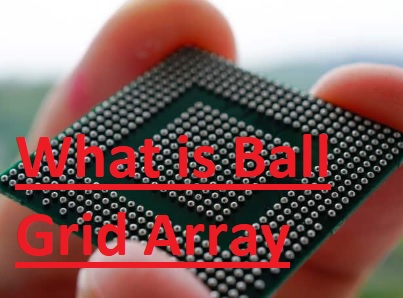
What is Ball Grid Array (BGA) on a PCB Board
06/20/2023 at 12:10 • 0 commentsHi, guys welcome to the new post. In this post, we will discuss What is Ball Grid Array (BGA) on a PCB Board. Ball Grid Array (BGA) is a packaging technology commonly used in electronic circuit boards that have different advantages than other traditional packaging techniques. It is popular due to its ability to accommodate larger interconnections in a small area, so it is best for high-density applications. In this post, we will learn Ball Grid Array (BGA), and other parameters. So let's get started What is Ball Grid Array (BGA)
What is BGA?
- BGA is a surface-mount packaging type where solder balls are configured in a grid-like pattern on the bottom of a component. These solder balls create electrical connections between components and the PCB board. BGA packages are the main part of microprocessors, integrated circuits, and other complicated electronic components.
[adinserter block="3"]
![What is Ball Grid Array]()
BGA vs. Other Packaging Technologies:
Feature BGA PGA LGA Package type Ball grid array Pin grid array Land grid array IC connection Solder balls Pins Solder balls Package size Compact Larger Larger Heat dissipation Good Fair Good Cost expensive Less costly Less costly Complexity More complicated Less complicated Less complicated Applications High-performance devices, devices with a lot of ICs thin devices, General-purpose devices, devices that do not need high performance General-purpose devices, devices that do not need high performance Advantages of BGA:
BGA has different advantages that make it the best for different PCB designs. Firstly, the small size package size allows for more components to be connected on the PCB, leading to higher functionality in a small area. 2nd, the shorter electrical paths between the component and the board improve signal integrity. BGA's thermal features also enable efficient heat dissipation, so they are good for high-power applications.
BGA Assembly Process:
The BGA assembly has different steps. It started with the application of solder paste on the board, followed by component placement with the use of automated machines. The PCB board then passes reflow soldering, where the solder balls melt and make reliable electrical connections. After cooling, the PCB board undergoes inspection to make sure proper alignment and solder joint quality.
Challenges in BGA Assembly:
BGA assembly also has unique challenges. The Main is the accurate alignment of the BGA component due to the absence of leads. BGA components also needed accurate control of the reflow soldering process to avoid problems like solder bridging and voids. With that, the inspection of hidden solder joints and the detection of defects pose additional problems
BGA Inspection and Testing:
Various inspection and testing techniques are employed to make sure the quality and reliability of BGA components. X-ray inspection is used to find hidden solder joints, while optical inspection systems can find defects on the component surface. With that, electrical testing, like ball shear, and ball pull tests, are done to assess the mechanical strength of the solder joints.
BGA Rework and Repair:
For faulty BGA components, rework and repair methods are employed. BGA rework does removing the defective component, cleaning the site, and replacing them with new ones. This process needs advanced tools and skilled operators to avoid damage to the board and adjacent components.
[adinserter block="5"]
BGA Reliability:
BGA packages provide high reliability due to their robust electrical and thermal connections. Though, some factors like mechanical stress temperature cycling, , and aging can affect their long-term performance. Accurate design considerations, material selection, and assembly methods are used to ensure the reliability of BGA components.
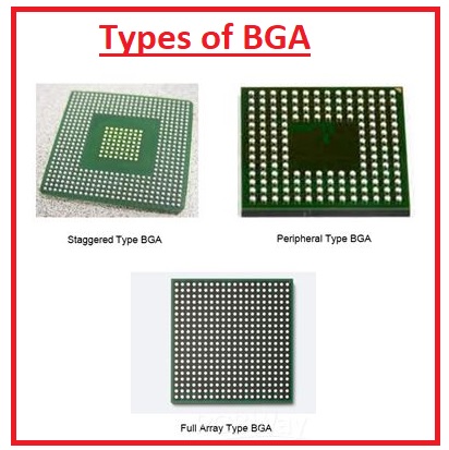
Types of BGA
![Types of BGA]()
1. Ceramic BGA (CBGA):
Ceramic BGA packages are made with the use of ceramic materials and offer excellent thermal properties and high reliability. The ceramic substrate has good heat dissipation,...
Read more »
This user joined on 03/15/2023.
 Lutetium
 slantconcepts
 kodera2t
 Alex Rich
 lion mclionhead
 vishal soni