 Ken Yap
I have a large pile of 4164 and 41256 1-bit wide DRAM chips from the PC era. Many of them were extracted from sockets or boards. I was curious to know how many are faulty. A web search quickly turned up many designs for Arduino based DRAM testers. Most of them required only a few extra components in addition to an Uno or a Nano. Wiring is also simple so I wired up a tester on breadboard.
(There are complex versions that test a larger range of chips (e.g. additional voltage supplies), and have fancy features like an onboard display, but this was a one-off task. For the same reason I have no interest in any of the published PCB designs for Arduino shields.)
The first design I wired up was this:
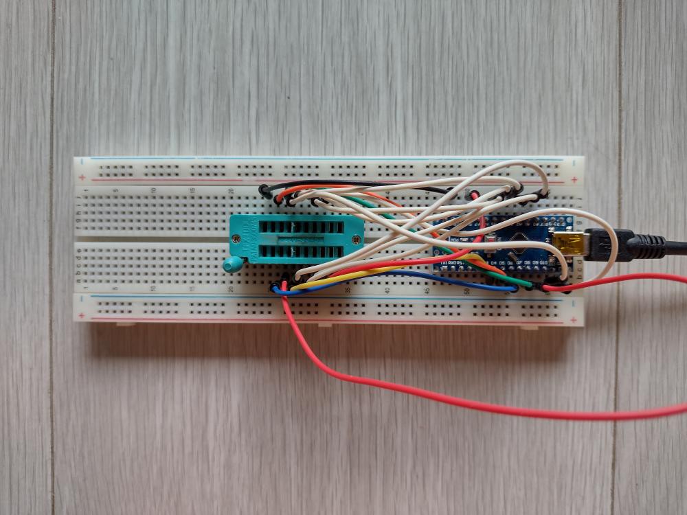
This worked well. I didn't even wire up the LEDs because the serial console displays the status. Each chip takes about 80s to test. For succeeding chips I just have to press the reset button on the Nano as the program is already flashed into the MCU. It found a handful of faulty chips. Interesting that a batch of Mostek chips failed the test. Either their specs don't work with this tester, or a process fault ruined the chips over time.
But this circuit didn't handle 41256 chips. So I turned to this design:
The wiring is different. Here they have tried to minimise wire crossings from each side of the Arduino to the chip socket, at the expense of a less logical pin assignment. But it doesn't matter since a table handles the mapping in the sketch.
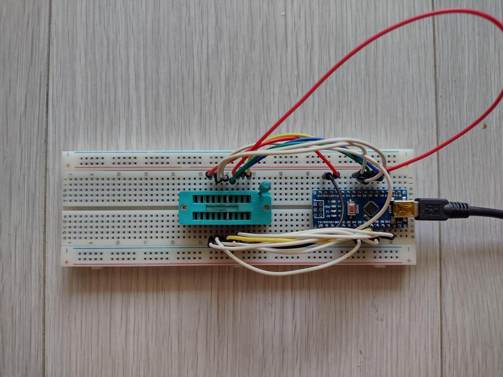
This also worked well. But with 4 times as many bits the testing time ballooned out to 288s. This meant many minutes waiting. There is only so much surfing I can do on the computer while waiting for tests to complete.
Hacking the sketch
I know that the Arduino library digitalWrite() and digitalRead() routines do a lot behind the scenes and this is reflected in the execution time. The Arduino documentation shows how to do direct I/O on the ports, but discourages it because for most sketches it doesn't matter and the sketch loses readability and portability. But the same page acknowledges there are situations where direct access is warranted. This testing sketch is just such a situation; it does a lot of bit I/O.
So I looked into how to rewrite the sketch to use direct I/O. A goal is to not change the structure of the code but use conditional defines to replace the digitalWrite() and digitalRead() routines.
For digitalRead() on the data out pin there is only one instance that needs to be replaced with inline code to read the pin, so that is easy.
Since writing HIGH or LOW are different code sequences in direct I/O, we define separate macros for the two situations, called dWH and dWL. When the optimisation is disabled, these map to digitalWrite(port, HIGH-or-LOW) and the program runs as before. When optimisation is enabled, these are defined as routines dWH() and dWL(). They use a switch statement to direct to the appropriate code for that pin. To discover the appropriate direct I/O statement one needs to consult the pin table of the Nano. The pins are also labelled in the sketch comments. So the overhead of direct I/O on a pin is a call, switch, and return.
Not all the digitalWrite() calls need to be substituted. Those dealing with the LEDs are not time critical and can be left as-is.
#define FAST_RW

#ifndef FAST_RW

#define dR_DO() digitalRead(DO)
#define dWH(p)  digitalWrite((p),HIGH)
#define dWL(p)  digitalWrite((p),LOW)

#else

#define dR_DO() (PINB & 1)

void dWH(int p) {
    switch (p) {
    case XA1:
        PORTD |= (1 << 2); break;
    case XA7:
        PORTD |= (1 << 3); break;
    case XA5:
        PORTD |= (1 << 4); break;
    case XA4:
        PORTD |= (1 << 5); break;
    case XA3:
        PORTD |= (1 << 6); break;
    case XA6:
        PORTD |= (1 << 7); break;
    case CAS:
        PORTB |= (1 << 1); break;
    case XA8:
        PORTC |= (1 << 0); break;
    case DI:
        PORTC |= (1 << 1); break;
    case WE:
        PORTC |= (1 << 2); break;
    case RAS:
        PORTC |= (1 << 3); break;
    case XA0:
        PORTC |= (1 << 4); break;
    case XA2:
        PORTC |= (1 << 5); break;
    default:
        Serial.println("Oops dWH"); break;
    }
}

void dWL(int p) {
    switch (p) {
    case XA1:
        PORTD &= ~(1 << 2); break;
    case XA7:
        PORTD &= ~(1 << 3); break;
    case XA5:
        PORTD &= ~(1 << 4); break;
    case XA4:
        PORTD &= ~(1 << 5); break;
    case XA3:
        PORTD &= ~(1 << 6); break;
    case XA6:
        PORTD &= ~(1 << 7); break;
    case CAS:
        PORTB &= ~(1 << 1); break;
    case XA8:
        PORTC &= ~(1 << 0); break;
    case DI:
        PORTC &= ~(1 << 1); break;
    case WE:
        PORTC &= ~(1 << 2); break;
    case RAS:
        PORTC &= ~(1 << 3); break;
    case XA0:
        PORTC &= ~(1 << 4); break;
    case XA2:
        PORTC &= ~(1 << 5); break;
    default:
        Serial.println("Oops dWL"); break;
    }
}

#endif
Timing the new code showed that the time was halved, to 154s, a dramatic improvement. The bottleneck remaining is the bit handling. For the innermost loop where the pins for the address are set up, this could be replaced by an unrolled loop for the 9 pins. But this goes against my intention not to change the structure of the code, only to switch implementations using a define.
It would be even better if a whole port could be written at once for the address setting. But unfortunately the AVR MCU used doesn't expose complete ports. Another dev board with whole ports would make this feasible.
The original sketch and my modified version are in this Github repository. If you do a diff you will see the lines I have added or modified. There are one or two small changes not related to the optimisation. Just one define can switch between the original and my code. You'll also see some other conditional code that didn't work out. It's possible that the back to back bit operations were too fast for the specified timing for the control lines of the DRAM.
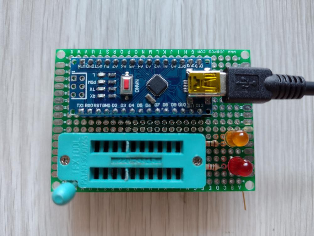
Along the way I made a dedicated tester using a prototyping board:
A batch of about 30 Samsung 41256s failed the test, except for 2. Who knows what happened, whether these DRAMs are marginal with the tester, the chips failed over time, or they were killed by the equipment they were in. It's not worth my while to investigate further.
An interesting observation is most of the 4164 chips had no solder on the pins but some of the 41256s did. It seems that early DRAM tended to be socketed for easy replacement. Only later did DRAMs become reliable enough to solder onboard.
Free chips! (but no fish)
All told I have about 150 each of good 4164 and 41256 chips. The irony is I can't think of anything I want to build with these as it would involve too much board space and soldering for a paltry amount of memory. And DRAM requires handling refresh. As far as I know restorers of old microcomputers and game consoles might use these. If you do this and live in Australia you're welcome to the pile of DRAM chips for free either by pickup or for the cost of postage. I'll even throw in the tester board (without the Nano and ZIF socket). PM me if you want the DRAM chips and tester. The chips have been taken, thanks for your interest.
Discussions
Become a Hackaday.io Member
Create an account to leave a comment. Already have an account? Log In.