 Christoph Tack
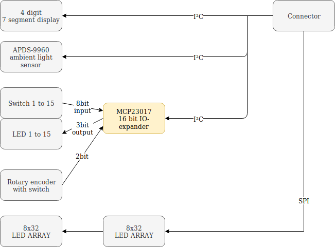
Block diagram
First layout idea
![]()
IO panel with two times two concentric LED rings
Nothing to be really happy with. This design is too large. There are three rotary encoders with an internal switch. The high switch actuation force of these switches prevents the panel from being used in a vertical position. You would top over the clock when you push the switch of a rotary encoder.
The three rotary encoders will each be replaced by a push button switch. There will be one encoder for general change of values. You push the switch to select that functionality. Using the rotary encoder you can then change the value at will. This kind of user interface is used on the R&S RTO200O series oscilloscopes.
The double rings of WS2812B LEDs are also eating up too much space. Let's replace these by LED bar graphs.
Second layout idea
The space consuming LED rings have been replaced by LED bar graphs. Each one needs 10 inputs, so it will take some effort to get these routed properly.
The button for setting the brightness of the LED array and the light sensor are not related to alarm settings, so they have been removed from this module. Functionality for setting LED array brightness should be physically located near the LED array, not on a separate IO panel.
So what's left?
- A menu button to cycle through the alarm settings (top left).
- top right: a button to set alarm hour & minutes
- seven buttons to enable the alarm for certain weekdays
- a button to set the brightness of the sun rise simulation with the corresponding LED bar graph.
- a button to choose the song to wake you + LED bar graph
- a button to set the music volume, with LED bar graph
- a single rotary encoder to change the value of a setting once the setting has been selected by a push on its button.
It all doesn't look to well: all those bar graphs... The rotary encoder is out of place.
Let's work out another idea...
Third layout idea
Why not incorporate the LED bar graph functionality in the LED array? We have plenty of pixels already there. Both sides of the LED array can be flanked with buttons. Alarm settings on the left, LED array settings on the right. The pixel row next to the button can be used as a virtual LED bar graph.
The LED array "PCB" and the clock-io-panel have been merged into a single PCB. This reduces cost and it will mechanical assembly easier.
Functionality overview at a glance, counter clockwise, starting at top left:
- setting brightness of sunrise simulation
- setting volume of alarm / music
- select alarm tone /song
- menu button for selecting the settings of alarm1 or alarm2
- seven buttons to enable/disable the selected alarm on a day of the week
- setting the alarm time
- setting LED array night brightness
- select at what ambient light brightness the day/night switch should occur.
- setting LED array daylight brightness
Alarm + LED array functionality merged into one IO panel. Connectors & ICs not yet shown
In the middle you can find :
- the LED array to show time & settings
- the ambient light sensor
- the rotary encoder to change the settings. The switch on the rotary encoder will not be used.
- seven segment display to show alarm time. It will only show the alarm time if an alarm is scheduled in the next 24 hours.
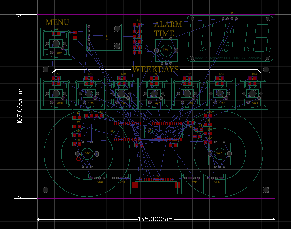
This clock-io-panel is bigger than the previous one, but 196x122mm will still fit on pretty much any night table.
Layout for PCB Revision 0
Some improvements with regard to the previous version:
- Switches moved to the edge of the PCB. On the previous version, there was no room between the switches and the LED array, which makes it harder to add a sturdy front panel later on.
- Grouping icons in groups of related functionality to improve intuitivity
- Changing some icons to make them more intuitive.
- Swapping led 7-segment with FFC & light sensor for ease of routing.
- Reference designators have been moved from topSilk to topAssembly layer. I don't want them to be visible on the PCB.
- Adding EMC filtering for the FFC.
Substantial effort went into the placement of the switches and LEDs so that as much as possible routing could be done on top layer. As such, the bottom layer is able to serve as low impedance ground plane.
Five pieces of this PCB cost me €14.32 + €9.03 shipping. Four of the PCBs will never be used. PCB costs dramatically increase when your design doesn't fit a 100mm square as in this case. If they had, the PCB would only cost me €1.
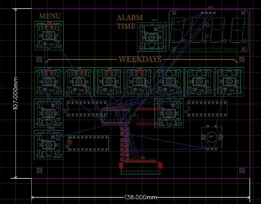
Revision 0 was all well and good, but the big clock IO panel PCB is relatively costly and won't find any usage in other projects. It serves mainly as a carrier for functionality that is already on modules (displays, light sensor). The fifteen LED/switch combinations might be split up in four identical sections of four switches each. There would be one module carrying only three switches. It would add cost in wiring and connectors, but this switch module could easier find usage in other projects. I would be able to use four of the five prototypes sent to me. These switch modules would also fit the 100mm square template of the PCB manufacturer. The different modules could then be mounted on a laser cut panel. A separate module would be needed for the rotary encoder. Buy them, not make.
Discussions
Become a Hackaday.io Member
Create an account to leave a comment. Already have an account? Log In.