 Christoph
I'm building a BLDC ESC based on
- EFM8BB2 running BLHeli_S
- NCP81253 Gate Driver
- SIZ322DT NFET pair
- and a DMN2990UDJ fual NFET for level shifting between 3V3 (MCU) and the 5 V gate driver logic
Link to current schematic (possible error in MCU to level shifter signals: pwm and com signals might be swapped so "Ap" should actually be "Ac", same for B and C signals):
https://s3.amazonaws.com/static.projects.hackaday.com/9684061580420948473.pdf
power FETs: https://www.vishay.com/docs/79370/siz322dt.pdf
gate driver: https://www.onsemi.com/pub/Collateral/NCP81253-D.PDF
NFETs for level shifting: https://www.diodes.com/assets/Datasheets/DMN2990UDJ.pdf
MCU datasheet: https://www.silabs.com/documents/public/data-sheets/efm8bb2-datasheet.pdf
MCU reference manual: https://www.silabs.com/documents/public/reference-manuals/efm8bb2-rm.pdf
I assembled a fresh board without the MCU:
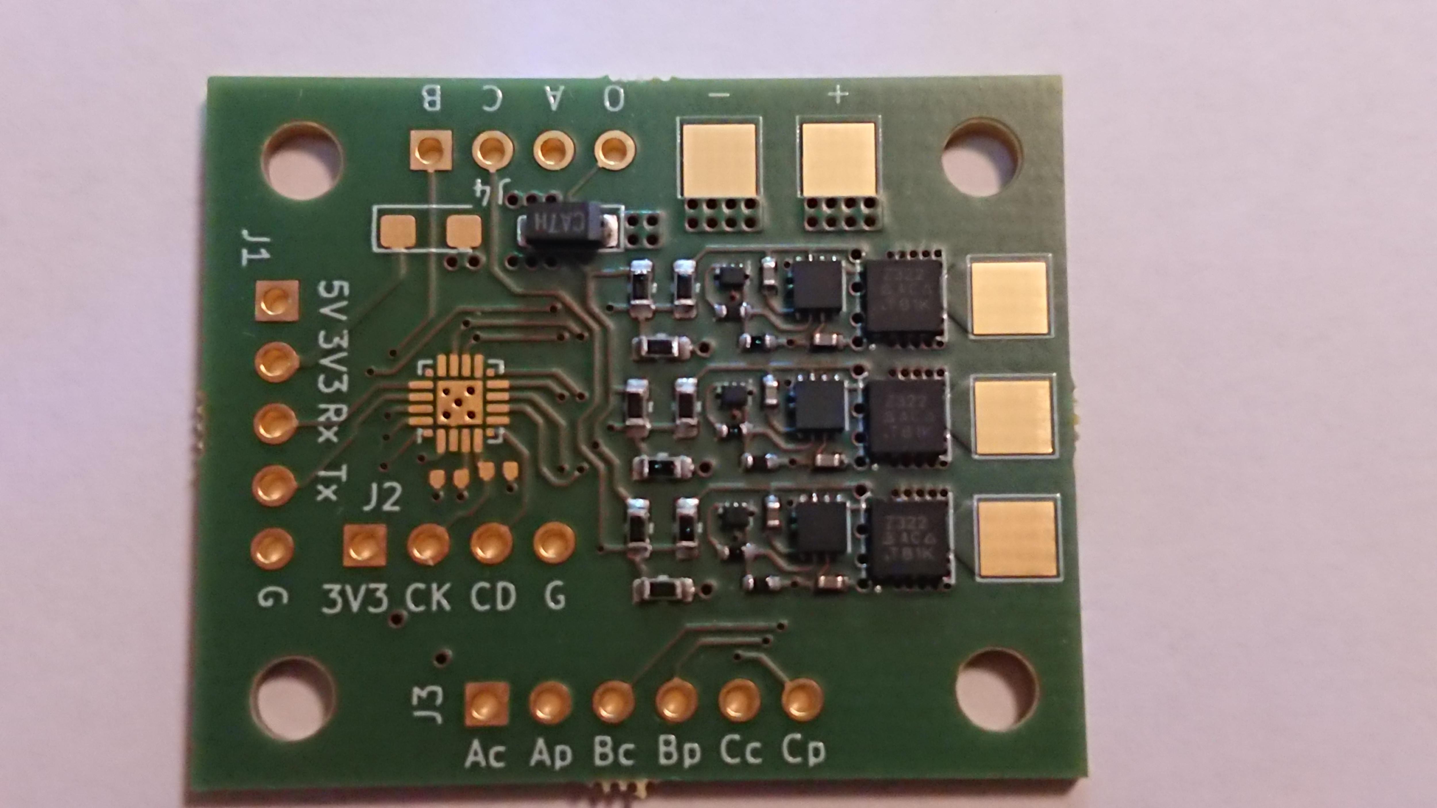
Measurements I've done so far to make sure the board is healthy (without powering it up):
- level shifter DMN2990UDJ body diodes show normal forward voltages and block in reverse
- power FET SIZ322DT body diodes show normal forward voltages and block in reverse
Older content:
As long as the MCU isn't programmed, it should be possible to inject the level shifter input from an external source.
Schematic of one half bridge driver:
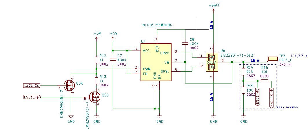
The level shifter is to the left (Q5, R12, R13), gate driver in the middle (U4, C7, C8) and motor driver FETs to the right with some feedback resistors (labeled "easy access" because I'm not sure about the values).
VBat can be between 2.5 V and 12.6 V (maybe 16.8 V) and I'm currently using a 2S LiPo charged to 7.5 V.
Gate Driver:
The gate driver will switch on the high side FET if PWM is high. It will switch on the low side FET when PWM is low, and it will disable both if PWM is somewhere in the middle.
Level shifter logic:
    Cc Cp PWM PFET NFET
1)  0  1  2V5 off  off
2)  1  1  0V  off  on
3)  0  0  5V  on   off
4)  1  0  0V  off  on
This makes the whole driver stage look like some sort of an imaginary PFET-NFET pair (line 4 in above table is an exception to that).
The problem
When I apply 0 V to Cc and 0 V to Cp, the high side FET isn't on. I can only measure some 3.8 V, but it should be VBat. It was pointed out in the hack chat that the gate driver might require PWM with a duty cycle less than 95% to work correctly, so I also tried with 24 kHz PWM and 90% duty cycle. Since Cc logic is inverted, I actually injected 10% duty cycle on Cc.
The above was measured with a multimeter.
Things look different with a scope
Input to level shifter and its output to the gate driver; Ch1: PWM to gate driver (5V logic), Ch2: input to level shifter (3V3 logic, signal Cp):
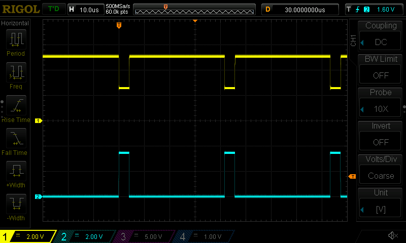
That the PWM signal (Ch1) is going to 2V5 instead of 0V is caused by the voltage divider (R12 and R13). The gate driver handles a 2V5 input by disabling both output FETs. Input Cc was low all the time.
The output of the gate driver can't really be accessed so I took a look at the output (testpad to the right in the schematic). Ch2 is still the 3V3 input, Ch1 is the testpad output:
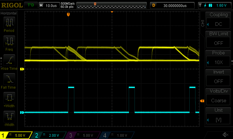
Indeed the output goes to VBat so the high side FET is switching on. It doesn't go down to 0V when off because the low side FET is never on.
Next steps:
- Connect Cc to Cp to have complementary output with the low side FET
- Add a light load to the output. Since I only have 1/4 W resistors, a couple of 680 ... 1K Ohm resistors in parallel should be fine.
Again thanks to Bharbour for helping.
That helped!
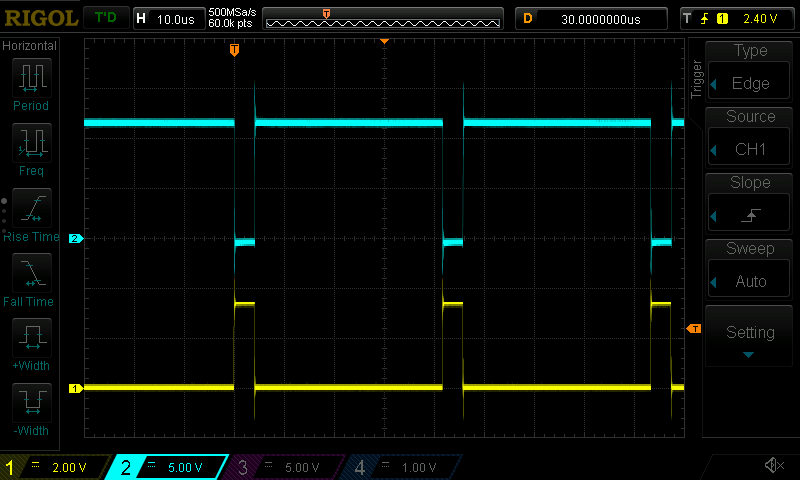
Driving both FETs and adding a load of 6 x 1 kOhm (lack of power resistors...) helped. The following screenshot was made with a 3S battery at 11.4 V, and that's what I'm seeing at the output. Ch1 is the input to both Cp and Cc, and Ch2 is the output at the motor pad:
Time to figure out how to program the on-board MCU.
Discussions
Become a Hackaday.io Member
Create an account to leave a comment. Already have an account? Log In.