mateusz.kolanski
-
We're not dead (yet...)
08/14/2016 at 20:35 • 0 commentsIt's been a long time, but I needed a break to stop going in circles, gain some distance, energy and new ideas to continue my struggle.
As you probably now, I've been using a modified MAME/MESS driver written for a handheld console called Game Master. As I started to play with it, I just wanted to have a way to see the DW-6000 firmware running, but as you know, the more you have, the more you want.
Yesterday I started to write my own MESS driver from scratch. It's not that complicated, once you know what are you doing. After a few hours I ended up with a working skeleton emulator with working (well, sort of) keyboard support and display.
I'm not going to show you anything now, because the keyboard works (very unreliably and somewhat random) just because of my mistake in coding (what do you know, sometimes it's a good thing) and after I fixed it, it stopped working. As I stated before it's probably because of the debouncing code in DW6000's firmware and that's something I need to investigate and understand now.
Apart from that I have a nice debugging tool which still needs some work to be fully useful, but right now it can do a thing or two.
So here's the plan for the nearest future:
- investigate how the debouncing routine works and 'fix' the keyboard support problem
- write a function that will be triggered by a press of a numeric key (1-8) and then it will watch the memory for a write of that value - that should help me track down the memory address which holds the number of a parameter or value we want to select
Keep the fingers crossed!
-
Also sprach DW6000
03/30/2016 at 11:06 • 2 commentsFinally, after numerous attempts I made this thing speak to me!
But first things first. Currently I'm trying to find the code responsible for scanning and analyzing the keypresses. And I want to do it the easy way (i.e. using the debugger, not by reading /and understanding/ the whole source code). How hard can it be? Harder than I thought.
Let's take a look at the schematics (I have merged two pages and removed some irrelevant connections).
![]()
The keyboard matrix is driven by port A and port B of uPD7810. The CPU sets a 4 bit value on PB[0..3] which then gets decoded by IC11 and IC12. As you can see, both IC11 and IC12 enable lines are tied together, but IC11 is enabled when PB3 goes high and IC12, when it goes low. So if we set a PB value between 0 and 3, we will put SW lines 8-11 low, while values 8-F are enabling SW lines 0-7. SW lines 0-7 are connected to the keyboard and 8-11 are connected to the switch matrix.
SW columns are connected to PA through non inverting buffers. They are pulled up, so if no switch is pressed, PA should read 0xFF. DW6000 stores switch states in the external RAM ($27E9-$27EC). Ok, so far so good. Now, I thought that if I modify those addresses (e.g. change $27E9 from 0xFF to 0xEF) I should see some changes on the displays (= display memory - $27E1-$27E6 for 6 digits and $21E7 for the LEDs), right? Wrong. Each time I modified that value, it came back to 0xFF after some time with no change on displays whatsoever. I tried to set some watch- and registerpoints in the debugger, but it wasn't useful, cause the debugger was halting code execution too often.
I started to browse the source code looking for the places where PA is being read, but there was still too many gaps (i.e. addresses in RAM that contain something that gets analyzed, etc.). OK, so I need some help. Maybe I could force MAME to emulate those keypresses somehow?
Looking at the sources I found, that there are special handlers for both reading and writing to the memory and ports. I have modified the gmaster_state::gmaster_port_r handler to return a fixed value (0xFE) each time PA is being read and PB is set to 3. That should emulate the up key. The code compiled and as expected I saw one FE among FFs. Nice. Unfortunately that didn't work either. I was confused. After numerous attempts to make this damn thing speak to me I modified the code to return 0x00 (all keys pressed) no matter what. And this time... nothing happened. But at some point I changed one of the stored PA values and after some struggle I saw some values in the display memory saying "TAPE". Great success! OK, now I get it. There must be some sort of debouncing code that samples PA value, holds it, compares, yada yada yada and finally does what it should. I don't want to bore you to death describing my failed attempts to make this thing work, so I just show you what I ended with:
READ8_MEMBER(gmaster_state::gmaster_port_r)
{
	UINT8 data = 0xff;
	static __attribute__((__unused__)) UINT8 cnt = 0;
	switch (offset)
	{
	case UPD7810_PORTA:
		if (m_ports[UPD7810_PORTB] == 0x00)
		{
			if (++cnt % 3)
				data = 0xEF;
		}
		logerror("%.4x port %d read %.2x\n",
                         m_maincpu->pc(), offset, data);
		break;
	}

	return data;
}
And that made me very happy. Looking at the memory window I finally saw some predictable changes: the value on the 1st display changed to 5- (1st keypress) and then to 55 (and so on).
Now I will try to "program" a sequence of keypresses which should bring me to an unsupported menu value. Wish me luck, I hope I'm getting closer.
-
Going live
03/23/2016 at 15:15 • 0 commentsToday's a big day for my little project - I decided to make it public. I still have some backlog (put a photo here and there, rephrase some sentences, etc), but I can probably take care about it later.
As for today's activities I set up a local GIT repository and committed some code. I'm not planning to go to github, because I'm reverse engineering proprietary code. I know that DW-6000 is an ancient piece of gear and I bet nobody would care, but still I don't want to turn my little project into a lawsuit :) *Maybe* someday I will contact KORG via korgforums, but not yet.
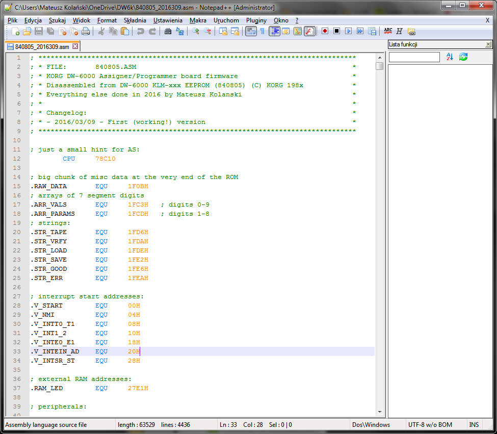
I created a custom Notepad++ style to highlight upd7810 syntax properly. It's far from being perfect (it doesn't color some hexadecimal values and doesn't support labels at the moment) and some colors are well.. at least questionable, but it's still a nice thing to have.
![]()
I managed to understand/comment some more source code. I focused on the main loop and timer ISR just to see what it does when it's "idling". It's still incomplete and somewhat convoluted and I got a feeling, that I'm nowhere near the end - but that's the beauty of assembly language - jump, branch, call and interrupt in the middle :)
-
09-11 march 2016
03/12/2016 at 18:32 • 0 commentsI started replacing some constants with nice labels, to make the code look more readable:
![That's my IDE]()
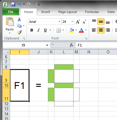
I made a simple excel sheet that converts hexadecimal values into 7 segment characters to be able to decipher some values at the end of the file.
![]()
Seeing "words" like TAPE, LOAD, etc gave me a few hints about how the code works. I also added some constants pointing to known places in external RAM.
Now it's time to spend some time with the MAME debugger. I have to look carefully at the routines doing something with PA/PB (keyboard reading) and those which use the corresponding data saved in RAM. I'm pretty sure that I have a rough idea about how they work, but I wasn't able to change anything on the displays (well... make the display memory to change to be exact) just by entering some values to where the switch memory is supposed to be. Long way to go.
The more I know about the inner workings of DW6000, the more worried I am about the available space in ROM (whopping 72 bytes - I think, that "project 72" would make a good name for this one). Right now I think (or better said I expect, because I didn't have a chance to verify this guess), that the parameter selection is performed on a base of jumps to subroutines (that's what the data at the end of the file is for?), where each combination generates an offset to a function pointer. If a given combination is invalid, the resulting pointer will invoke this same subroutine which just waits for another, valid keypress. If it worked this way (i.e. one jump address per combination), it would be possible to modify some jump addresses without wasting precious bytes. If not (i.e. the code check if the keypress is in a fixed range), things will get more complicated.s We'll see. My other concern is, that since PORTB is partially used for row addressing (you know what I mean) and I want to use its second half for extra memory addressing, I will have to make sure, that the existing code which "shares" PORTB will do the masking first. And that means some extra code.
It turns out, that my little project brings other people's attention. I was explaining my idea to a fellow geek and he suggested, that I could (or even should) use a latch driven by PC2 or PC4 (right now I feel that I might need both of them...). This way I won't have to think about preserving PB's value between function calls. Great idea. Might give it a try, although I like to keep things (look ;-D) as simple as it gets. He also suggested that I could profit from constructing a simple device emulating my ROM chip, something like an SRAM chip with serial programming interface. Another good idea, definitely worth considering.
I could really use a kind of versioning system since now I'm dealing with some proper source code:) All you wish me luck and keep the fingers crossed.
-
- march 2016 -
03/12/2016 at 18:32 • 0 commentsI'm more and more convinced, that I can't do much without an assembler. I have even started to read some theory behind the inner mechanisms of assemblers because I might end up writing my own one. (timelapse) Oh, no - that won't be necessary (well, maybe someday I will try to write my own one, just because of fun and things you can learn), there is one called "The macro assembler AS" written by Alfred Arnold (huge thanks about that!) which fortunately supports NEC 78(C)10 microcontroller family! Now that's what I call luck. Anyway, it won't be that straightforward, because the unidasm syntax is a little bit different than the AS' one. So, the story begins...
First of all I started to write down all the things that must be done in order to assemble the file:
- find a way to do the jumps and calls properly
- decode all the jump tables and data
- fix malformed opcodes (resulting from the disassembly of data)
- find a way to put some code (like interrupt vectors) where it belongs
The first task was rather easy - using some regular expressions I have converted the addresses in front of each line into labels - shortened them to 16 bits, added a leading dot and trailing "H" (H for hexadecimal, more syntax conversions later) and a colon (00000000 -> .0000H:). I have also moved the hexadecimal macine code values to the very end of each line turning them into the comments. I will need them to decode jump tables and other data later. After such conversion, each line looked more or less like this:
"00000008: 54 FF 00 JMP $00FF" => ".0008H: JMP $00FF ;54 FF 00"
The next thing to do was to convert jump addresses into labels aswell. The one reason is, that AS requires labels for jumps and calls (I'm not sure about that, but let's leave it this way), but what's more important, this way we can assure, that we don't have to deal with hardcoded addresses anymore. Neat. Another regex, another success:
".0008H: JMP $00FF ;54 FF 00" => ".0008H: JMP .00FFH ;54 FF 00"
AS can adapt to multiple numbering formats like $0000, 0x0000 or 0000H but I have chosen to convert all the numbers from Motorola ($0000) into Intel (0000H) syntax (just because, according to AS manual, NEC used this format). This didn't go as well as I thought, because I had to convert some numbers manually.
Ok, so far so good. Let's do the next point on my list. Decoding jump tables (fortunately not that many) either involves programming some heuristics or just using the CPU between your ears. The human brain can spot some patterns and regularities much easier than a piece of software. Basically there are 2 possible uses of the TABLE opcode:
1. to prepare the jump address which will be executed using the following JB opcode - in this case you have to validate to which point the data makes sense - this is a little bit tricky, especially in case of very long jump tables
2. to store a value in the C register used for example as an offset for something - that's easy, because in most cases, the next opcode after TABLE is a JR to where the data ends, apart from that this data comes mostly in sequences, so it's rather easy to spot.
After I have figured out where the data ends, I have converted it into the series of "DB" directives. This time it was all done manually and, what I realised later, I have done only one small mistake (I can't remember if I typed the same data twice or just skipped a part of it).
Sometimes it was necessary to adjust some opcodes - unidasm can't distinguish between data and code so in some rare cases the first byte after table data was merged with the last byte of data and decoded incorrectly.
Ok, now it gets really interesting - there's a bunch of "stuff" at the very end of file, you can't miss it, because it comes after a series of FF's (which indicate an empty space). I have no idea what kind of data it is, but I'm pretty confident, that it's actually data - I was able to spot some 7 segment stuff and series of sequential values. So I decided to convert it into long series of DB's.
The next task was a piece of cake too, just put some ORG directives, and you're ready to go.
After a (long) while, the code started to look like it should. I have written a short python script to remove some of the labels created at the beginning. I have created a list of labels used by jumps and calls and told python to remove everything else. And it worked.
Finally I have tried to assemble the code. Of course it didn't work:) That's because of how the unidasm decodes the "zeropage" instructions. Its syntax denotes it by adding a "VV:" string in front of an operand (e.g. "LDAW VV:EE"), while AS (and probably everything else) requires following syntax: "LDAW EE". The next thing after, again, next failed assembly was to convert the names of register pairs (HL->H, BC->B etc.) and that was pretty much everything to make AS (or us) happy:) Of course the resulting binary file was a little bit (or more bits) different than the one before disassembly, but after spoting and fixing some typos (missed a line here and there, added some extra code, forgot to add an H after a hex value etc.) I have finally reached the point where the code was looking just how it should. Kudos myself.
-
- someday in 2016 -
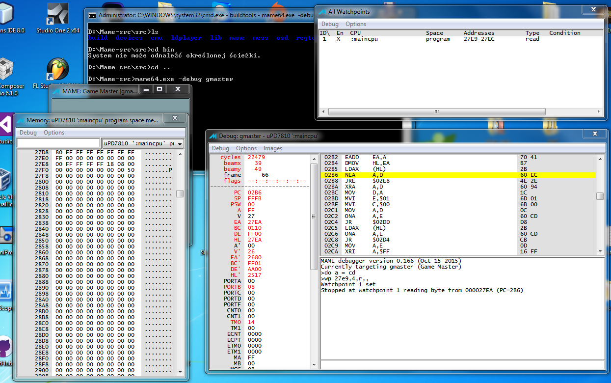
03/12/2016 at 18:30 • 0 commentsAfter a longer break I got back to upd7810 stuff. This time I changed my approach a little bit. First of all I have found a way to debug the code using (slightly modified) mame debugger - as I stated earlier, NEC 7810 was used in a rather unpopular handheld console called Hartung GameMaster (it was planned to be a GameBoy killer, but things went a little bit different I guess). All I needed to do was to modify the ROM size and declare remaining 56kB as read-write space to enable memory mapped IO. Apart from that I have enabled PORTA-PORTD to be visible in emulator and I was ready to go. Working with MAME debugger is somewhat similar to working with gdb - once you learn the syntax, it becomes a really powerful tool. I was able to trace some code visually, set some break- and watchpoints on memory locations of my interest and this way I figured out some more memory locations which hide data I was looking for.
![]() Note: I cheated here just a little bit - as you can see, I'm watching addresses from $27E9 to $27EC where probably key presses are saved. That's one of my most recent findings, but back then I didn't have a clue about that:) Just trying to make it look nice.
Note: I cheated here just a little bit - as you can see, I'm watching addresses from $27E9 to $27EC where probably key presses are saved. That's one of my most recent findings, but back then I didn't have a clue about that:) Just trying to make it look nice. -
Day 5
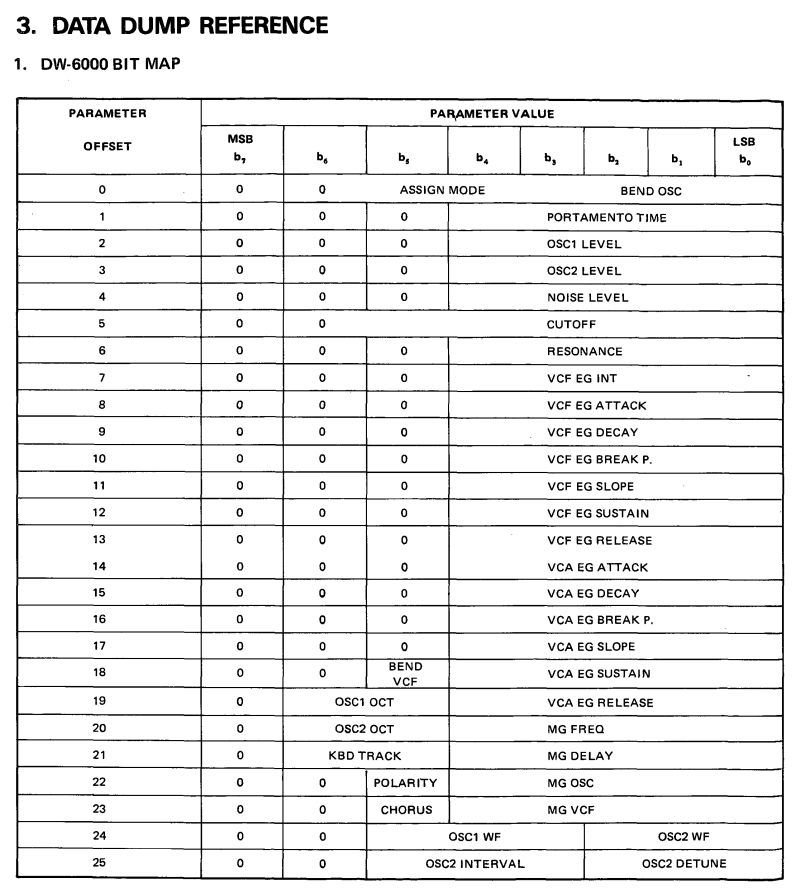
03/12/2016 at 18:29 • 0 commentsMore assembly reading today. And some findings too. There are 64 patches, each of them is 26 bytes long (I figured it out the hard way - by reading the save/load routines, but this number and the internal patch structure is described in the service manual, d'oh!), 0x2000h is the patch #0 address as well as the beginning of ext-RAM, next free address (0x2680h) is the "working patch" address, i.e. where the currently edited patch parameters are stored. BTW, if you look at the patch structure, you will see that there's no single parameter or parameter pair which occupy 4 bits at most:
![]()
So if I'd like to add the new bank parameter, I either have to do it using two addresses (to store two 'high' bits and two 'low' ones) or to reduce the number of banks to 8. But the bright side is, that I'd be able to store the bank numbers along with the patches. Neat! I started to draw a RAM memory map, but I still have too many gaps.
-
Day 4
03/12/2016 at 18:29 • 0 commentsI figured out the following:
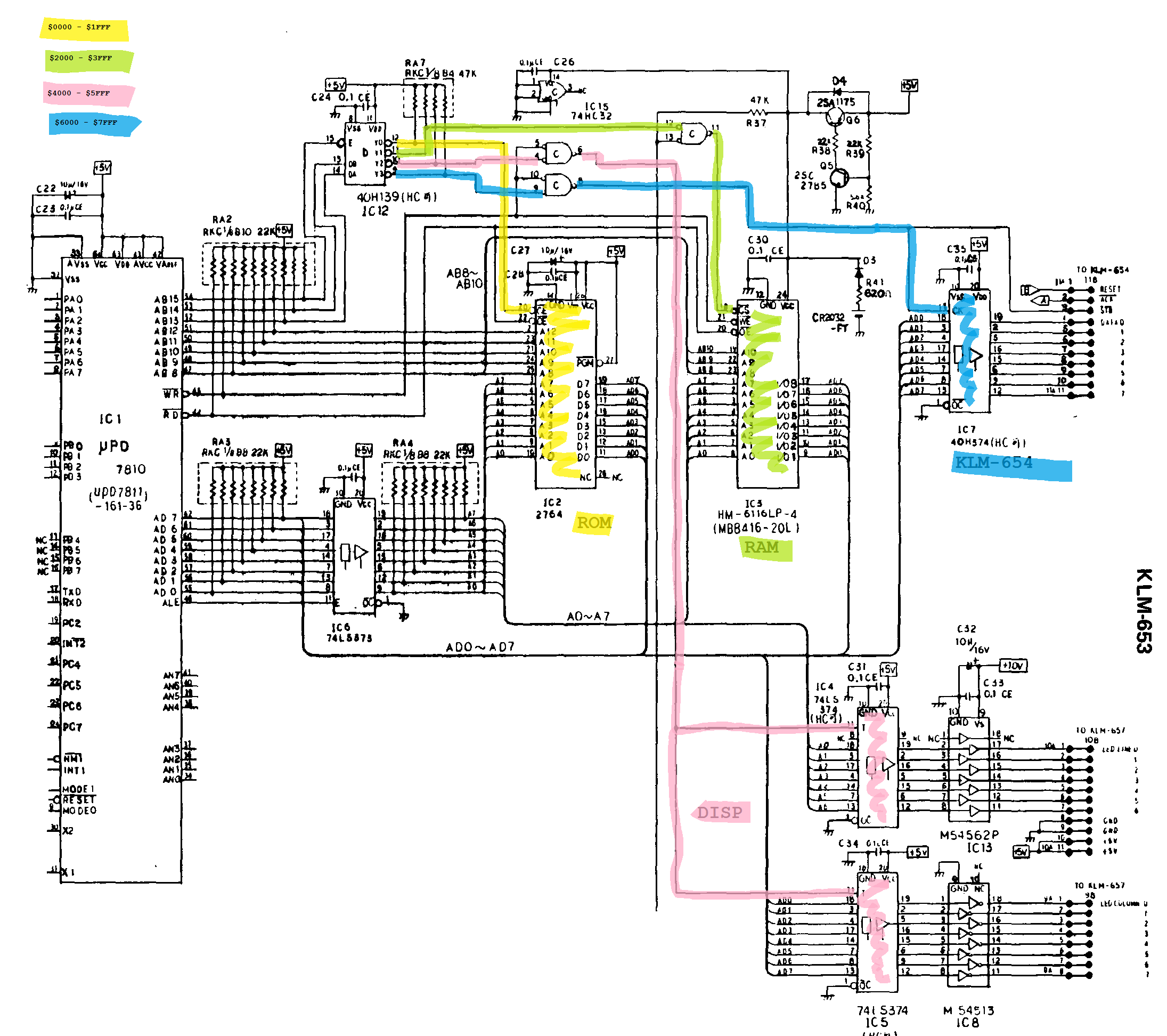
0x0000h - 0x1FFFh external ROM 0x2000h - 0x3FFFh external RAM (battery backed up SRAM) 0x4000h - 0x5FFFh LED displays 0x6000h - 0x7FFFh KLM-654 0x8000h - 0xFFFFh probably unused - setting the 16th bit high disables IC12, so no other chip is enabled - need to check this. The schematic below (I've removed some non critical circuitry just for readability) shows how it works:
![]()
With this information I noticed something else - there are a lot of writes to the external RAM during operation, so it means that the "working" patch values are stored there. What does it mean to me? Well I hope that there are at least four free bits somewhere (ideally four free bits per each patch) where I could store the bank number.
Right now I can try to roughly estimate what needs to be done:
- Find the place where the key presses are scanned and analyzed (i.e. only certain combinations are allowed)
- Extend it by adding one combination (e.g. 14)
- Allow to change its value within a 4 bit range (1-16)
- Store the result somewhere in the RAM
- Set the upper nibble of PB as requested.
Additionally: modify all the operations which affect PB to leave upper nibble untouched.
Looks as it could work, I only hope not to run out of memory... There are some FFs in the ROM but I don't know anything about the internal organization of RAM though. Furthermore I have this bad feeling, that at some point I will end up writing my own assembler or some kind of program which will help me deal with the jump addresses (they're going to change if I add/remove some code).
-
Day 3
03/12/2016 at 18:25 • 0 commentsToday I made another discovery: those addresses like 27c1, 2800 etc. If you take a closer look at the memory configuration you will see, that the processor uses the whole port F as an address bus and port AD as address/data bus. BUT there's only 8kB of ROM connected to the CPU! Yeah, that must be it. Let's take a look at the schematic. Bingo! Lines AB13-AB15 (aka F13-F15) are connected to IC12 (40H139) which selects RAM, LED drivers or the output buffer to KLM-654 depending of the state of its inputs, the E pin and the /WR line of the CPU. If neither input is selected (i.e. lower addresses are used), IC12 pulls down the /CE pin of the ROM chip enabling it for normal read operations. Sooo, if we try to write to addresses above 2^13 (0x2000h) we will end up outputting the data somewhere else. Probably.
-
Day 2
03/12/2016 at 18:24 • 0 commentsI found the Holy Grail: THE manual. Over 400 pages long epic journey through the innards of 7811. Neat! It was soo sexy that I even printed it out. And what do you know, I found an explanation for those illegal opcodes and other instructions making no sense whatsoever: there are two nice opcodes: TABLE and JB. The first one puts the current value of program counter incremented by 3 and whatever lies in the accumulator into the C register and does the same (but this time +4 instead of +3) with the B register. The latter instruction performs a jump to the address pointed by the register pair B:C. So basically if there is any data after TABLE and JB opcodes, it's the jump table - not instructions. That's why some of them were senseless and others illegal.
00000E8E: 48 A8              TABLE
00000E90: 21                 JB      		; jump to addres pointed by BC
00000E91: 29                 LDAX    (BC)	; if A = 0, jump to $1429
00000E92: 14 05 14           LXI     BC,$1405	; if A = 1, jump to $1405
00000E95: 5C 14              BIT     4,VV:14	; if A = 2, jump to $145C
00000E97: B8                 RET     		; ...
00000E98: 14 06 0F           LXI     BC,$0F06	; ...
00000E9B: 06                 illegal 		; ...
00000E9C: 0F                 MOV     A,L
00000E9D: 06                 illegal
Project 72 - Korg DW-6000 wave memory expansion
An attempt to reverse engineer and modify Korg DW-6000s firmware in order to expand its wave memory.

 Note: I cheated here just a little bit - as you can see, I'm watching addresses from $27E9 to $27EC where probably key presses are saved. That's one of my most recent findings, but back then I didn't have a clue about that:) Just trying to make it look nice.