 Ted Yapo
I'm not sure everyone agrees with my estimate of 39% efficiency for the 1.0 version. A rough SPICE simulation (with a different, possibly very dissimilar LED) showed 50%, but I'm inclined to believe the lower figure. Here's what I think is the problem:
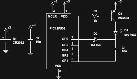
In the version 1.0 schematic above, the peak current through D1 is mainly limited by the Vce of the transistor and the impedance of the GPIO pins abused as current drivers. The measured pulse current is 102mA, and the LED forward voltage is 2.52 V. C1 probably gets charged to within 250mV of the battery voltage, nominally 3V, since the Vf of Schottky D2 is very low once the initial charge current falls. Let's assume then, that the total voltage available during the discharge pulse - with C1 effectively in series with the battery - is 2x3-0.25 = 5.75V. For the LED to only pull 102 mA, there has to be another 5.75 - 2.52 = 3.23 V dropped across the transistor, the ESR of C1, and the GPIO pins. That's an indication that the LED pulse is less than 50% efficient right there. In fact, based on this logic, the pulse is only 2.52 / 5.75 = 44% efficient. I assume the difference between the overall measured 39% and this 44% estimated just for the LED driver is due to the power consumed by the PIC and R1, which aren't accounted for in this analysis.
Assuming this is all true (let me know if you don't agree), what can be done to improve the pulse efficiency? It seems like the three possible culprits are C1, Q1, and the GPIO pins. C1 is an SMD ceramic cap, known for low ESR. I'm using either 2N4403's or ZTX718's, so I don't think the Vce of the transistor will be that large. That leaves the four paralleled GPIO pins. Oh, what the heck, the scope is right here...
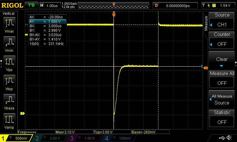
This is the voltage at the four paralleled PIC GPIO pins during the 3us pulse. When the pins are high, the voltage is 2.990 V (not a brand-new CR2032 battery). During the pulse, there's an initial negative spike (the LED ramp-up seen in earlier plots), then the voltage levels off at 1.580V - ideally it would be zero. There's half of the inefficiency (i.e. half the 3.23 V of "mystery" drop).
Here's the voltage at Q1's collector during the pulse:
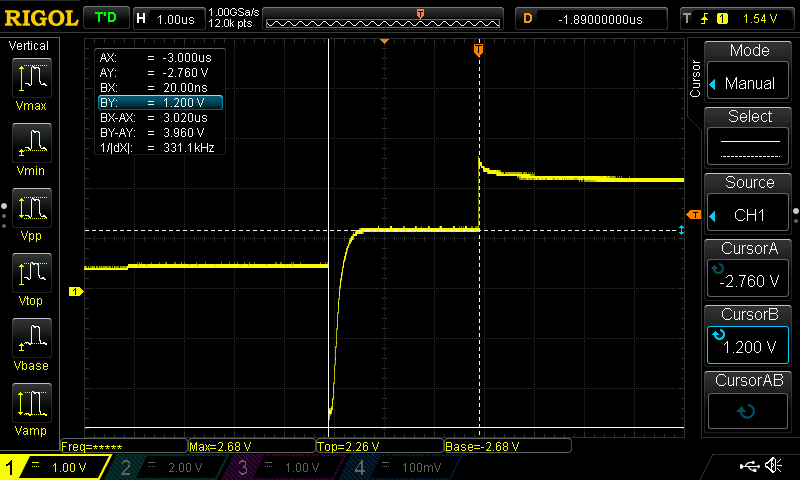
The initial negative spike drops to -2.76 V. This sounds like my estimated 2.75V charge on C1, now connected "backwards", pulling the collector low until the current pulse ramps up. After the initial transient, the voltage at Q1's collector stabilizes at 1.2V for the rest of the pulse. This means the transistor is dropping 2.990 - 1.2 = 1.8V. This is really surprising - it suggests that Q1 is starved for base current and not in full saturation during the pulse. I'm going to have to think about that a little. If true, it does explain the 3.23V drop, though: 1.8 + 1.59 = 3.38. There's an extra 150mV of measured drop, but my estimate for the charge on C1 could easily be that far off.
Whatever the reason, this analysis would appear to support the notion that a lot of efficiency is disappearing into the high and low side drivers. The knee-jerk reaction would be to replace both of them with low-Rds MOSFETS. But, what happens then? Without the ballasting provided by the (lousy) existing drivers, the LED current will be excessive (the datasheet shows a Vf of only 3.1V at 1000mA), causing the required pulse width to decrease even more, which isn't practical with the PIC timing. Moreover, the initial spike behavior (which I think is due to the LED junction capacitance?) above would consume a larger fraction of the pulse time. Finally, this would be close to driving the LED with a voltage pulse, instead of a current pulse, and the resulting power will have a large temperature dependence, and will vary from LED to LED just based on Vf spread.
I have an idea about what to do. I'll write it up in the next log. Tonight - I can't sleep.
Addendum 2016-08-06
I woke up realizing why the Vce on Q1 is so large. The GPIO drivers are also responsible for the gate drive on Q1. When the low-side drivers get pulled up by the current pulse, this reduces the drive on Q1's base, and keeps it from delivering enough current. I could try using 3 paralleled GPIO's for the low side, and give Q1 its own line, but then the drop on the low side would be even worse. It might be a worthwhile trade-off.
Discussions
Become a Hackaday.io Member
Create an account to leave a comment. Already have an account? Log In.