 Yann Guidon / YGDES
I have a problem since the beginning. At least for the relay version, and probably others, the register set uses two MUX8 and one DeMUX8 per bit. This creates a fanout of 1 for the LSB of the address, but a fanout of 4 for the MSB (or vice versa). There is a very significant imbalance and the LSB drives 16 relays, while the MSB drives 64 relays !
The consequence is the increase in latency for reading operands (write decoding can overlap the execution). The LSB level can be switched quickly (FO=16) but the MSB level requires amplification stages, which delay the signal.
Ideally each address bit should drive one third of the MUX2. The numbers have decided otherwise : 16+32+64=112 (=16×7), there is no 3 as factor and 112/3=37.333... That's very inconvenient. But I have found that it's possible to approximate this goal with the help of some bit shuffling.
Let's remember two of the design constraints (at least for the relays) : all the bitslice are identical and a whole MUX level can't be split (on each board, or else this increases the routing complexity). As a consequence, an address bit has a "fan-in" of 1, 2 or 4. The trick is to send the 3 control signals to (globally) equal amounts of fan-in.
This means that each address bit will drive the MUX2 stage, the MUX4 stage and the MUX8 stage equally, or in other words : each bitslice receives a rotation of the address vector.
    MUX2 MUX4 MUX8
 0   0    1    2
 1   1    2    0
 2   2    0    1
 3   0    1    2
 4   1    2    0
 5   2    0    1
 6   0    1    2
 7   1    2    0
 8   2    0    1
 9   0    1    2
10   1    2    0
11   2    0    1
12   0    1    2
13   1    2    0
14   2    0    1
15   0    1    2
There is obviously a problem with the last line, because 16 has no common divisor with 3.
Another problem is specific to the relay implementation, using the CC-PBRL method: each "high voltage string" has 8 relays, two groups of four with the signal injection in the middle. This constrains the design even more but it almost matches with the current situation.
A "high voltage string" can drive one FI4, one FI2 and one FI1, this amounts to 7 relays. The 8th relay can be simulated by a resistor and bitslices become naturally grouped by 3 :
            M2 M4 M8
bitslice%0   a  b  c
bitslice%1   b  c  a
bitslice%2   c  a  b

a = b = c = 1 + 2 + 4 = 7 fan-in
This regular pattern helps design the drive logic and estimate the complexity.There would be 5 identical blocks of 3 slices, plus the last part. This requires a buffer with fanout of 5+1=6 (which can be done with a high-voltage string of 8). Since there is an identical buffer for every level, the latency is identical and all the bits arrive at the same time.
Yet this does not satisfy me because a string must have 8 relays, not 7. If the last relay is replaced with a resistor, 1/8th of the power gets wasted and this is not insignificant...
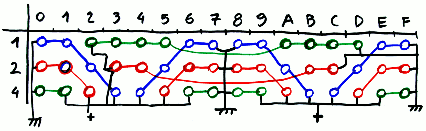
I found a much better circuit, which is explained with the simple diagram below:

Each group of 4 bitslices (wich evenly divides 16) has the same organisation (they can be mirored for convenience). Each bitslice has exactly one occurence of each color.
There are three full "long strings" of 8 Fan-In:
- 4-4
- 2-2-4
- 1-1-2-4
All these long strings have a "middle point" where the signal can be injected.
The remaining strings (1-1 and 2) can be assembled into a long string each, and it is just perfect (2-2-2-2 and 1-1-1-1-1-1-1-1) both in length and halvability.
Conclusion : the balance is not perfect but still quite good:
- 4 strings of blue
- 5 strings of green
- 5 strings of red
It's certainly a bit more complicated than the initial fanout tree but no power is wasted in resistors. The fanout of 4 can be handled by 2 low-voltage CCPBRL (4 relays). I'll have to see if the CCPBRL can handle a fanout of 3, so the case of 5 can be handled with 2 and half low-level CCPBRL (5 relays and a resistor).
Finally, the layout of the bitslices is not changed : the coils of each
level are wired in series (on each board) and the connector does not need to provide direct access to each and every relay with a
pair of wires. This keeps the design compact.
The only requirement is to use the same pattern for the write MUX and the read MUXes, otherwise data written to one location will be read back on a different location...
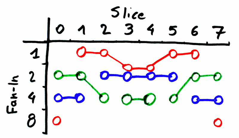
For the (D)RAM address lines, a similar approach is possible. It only depends on the configuration.
- For 512 words, the rows have 3 bits (on the bitslice) and the columns have 6 bits (=64 wires on the backplane). The bitslices contain a MUX8 that uses the above pattern for the backplane.
- For 256 words, the address bits are split in half, 4 bits go to the bitslice in a different pattern. Unfortunately the highest level has a fan-in of 8, which is the maximum a long string can drive, and there are 16 of them (more than 8), requiring a 2-levels fanout tree instead of one...
A 4-deep tree is a different beast but should be possible. The total fan-in is 1+2+4+8=15, 15×16=240 relays. For an even fanout, 240/4 address bits=60 outputs per address bit, which is right under 8×8=64, so a single buffer level is required. The number has many small factors, which makes me think it's possible to make a nice, symmetrical fanout-tree.
At first, I tried to play with different degrees of symmetry because I calculated that there had to be 15 strings for one half of the 16 slices.
Total fan-in: 15×16=240, 240/2=120, 120/4 address bits = 30
But 30 is not a multiple of 32, so the bits are split as 32-32-32-24 (or 4-4-4-3 strings of 8 each). The groups of 4 are inherently symmetrical but the group of 3 is a symmetry axis so I started avaluating all the possible arrangements (3) for 3 strings of 8:
Of those combinations, only one is viable : the red one touches the fanin8 signal (twice) while the others don't. It's a good starting point because the others would force the 3 other "colors" to access the FI8 input twice. Then I played with the combinations, using the red pattern as a basis.
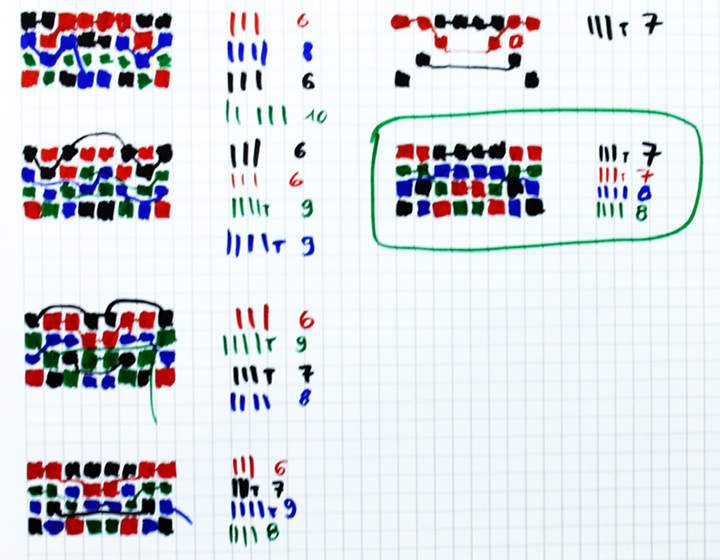
I used a few heuristics but after the 4th attempts (bottom of left column), it appeared that the initial estimate did not work. The guidance of having one group of 6 strings "pushes" the other groups into having more strings than 8.
I relaxed the initial constraint to 7 strings (that's 3 and a half strings for 8 slices) and after a failed attempt, found one solution (in the green box). Expansion is easy with a simple duplication of the neighbours :-)
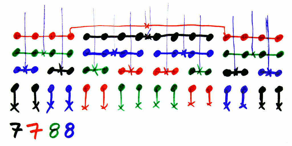
To me, it's quite beautiful and instead of having 8-8-8-6, we have a more balanced 8-8-7-7 (so only a couple resistors will waste energy).
Actually, the remaining fanout can be used for the parity DRAM bitplane.
Question : how does one handle a 17-wide fanout tree with 5 address bits ?...
Discussions
Become a Hackaday.io Member
Create an account to leave a comment. Already have an account? Log In.