A month ago I had never typed a line of C. Concepts like pointers, structs and treating variables as actual blocks of memory rather than abstract values were alien to me. But I really wanted to get into C; I knew that knowing the language would be vital for this project and there was only so long that I could put off learning it. I needed a target.
---------- more ----------
Karl had already written a Windows app in C# that would extract files from an image of an SSD. The Flash format had been well documented by the fantastic Clive D W Feather in his invaluable collection of SIBO documentation known as The Psionics Files. So I decided to follow in Karl’s footsteps and write an SSD file extractor in C. Something that would be more portable than his C# app, that I could compile on Linux, *BSD, macOS and Windows. And so, armed with a copy of the second edition of K&R and a few pre-ripped SSD images, my journey began.
I attempted to stick to C89 as closely as I could, only venturing into C99 when I really needed to. The one exception to this was for comments, where I used “//” liberally from the start. Three weeks later I had something that actually worked.
It compiles and runs on all the platforms I’ve mentioned above using both gcc and clang. Why both? Because it turns out these different compilers will pick up on different problems with the code, which helped me to write better code. I’ve also included pre-compiled apps for Win32 and Win64, which I compiled on Linux using MinGW32 and clang.
Obviously this is 100% alpha-quality software. The usual thermonuclear war caveats apply. It works for me, but you’ll have to let me know if it works for you.
Also, this might not work for you at all simply because you don't have any SSD images. Fret not! This will be remedied in the coming months. Karl has written an Arduino sketch that dumps the contents of any SSD via serial. It needs some more work to make it user-friendly enough for prime time, but once that's done we will be publishing it here. So, keep your eyes peeled!
Ever since the start of this project, the SIBO Serial Protocol (SIBO-SP) has loomed large as Something We Need To Know About. It's a protocol using 12-bit packets, a LSB-first data payload, and a series of reset and select control commands, all done on one data wire and one clock wire. As you'll see in previous logs, we've managed to decode a large amount of it and I've published my Sigrok decoder on my GitHub page.
The next step with the development of the decoder (and therefore the research into SIBO-SP) is the Slave Select Select Control Packet (SSel). Basically, how does a SIBO/EPOC16 machine know what it's talking to?
---------- more ----------
"Select" is kind of a misnomer, because in actual fact it's a question. The SIBO/EPOC16 device has a list of device IDs it knows how to speak to. Although these device IDs refer to specific ASICs and their modes, it's also possible to think of an ID as an ASIC's "language", For example, ASIC4 can "pretend" to be ASIC5 in Pack Mode. More on this later.
This SSel packet contains an ID number. This ID number refers to one of a number of different ASIC chips that could be in a slave device. Here's a list of the device IDs we've found so far and the devices they refer to.
ID
Name
1
ASIC2 Slave
2
ASIC5 Pack Mode
3
ASIC5 Peripheral Mode (“ASIC5 Normal” in OSSIBO.INC)
4
ASIC6 (undocumented, mentioned only in OSSIBO.INC)
5
ASIC8 (undocumented, mentioned only in OSSIBO.INC)
6
ASIC4
48
Unknown (undocumented, detected on Workabout mx)
56
Unknown (undocumented, detected on Workabout mx)
Each SIBO/EPOC16 device has a list of IDs it can speak to. When a SIBO-SP port is initialised, the SIBO machine first sends a "Reset All" command. This tells all slaves to stop what they're doing and listen for a SSel packet. Then, the SIBO/EPOC16 device goes through its list of IDs, starting from the top. It asks the slave, "Do you speak ID:x?". If there's no reply, it goes to the next ID on the list until it gets a reply or runs out of IDs.
The list of IDs is different for SIBO Serial Ports and SSD ports. This makes sense - the types of device that could be connected to a SIBO Serial Port are different to what would be put in an SSD port. However, the different types of SSel IDs that each device sends are interesting.
This is a list of SIBO devices with the IDs they send out on each port. Anything marked "unknown" is because I haven't been able to test it yet (I don't own an MC200 or Workabout 1MB and I don't have the right connectors for the MC or Workabout ranges).
Model
SIBO Port
SSD Port
MC200
Unknown
Unknown
MC400
Unknown
2, 1
Series 3
3, 5
2, 1
Series 3a
3, 5, 6, 2, 6
6, 2
Series 3c
N/A
6, 2, 3
Series 3mx
N/A
6, 2, 3
Workabout
Unknown
Unknown
Workabout mx
Unknown
48, 6, 2, 3 1
1Wmx also sends ID:56 at boot on the SSD port whether the door is open or closed.
What's interesting is that for every SSD port I could test, it asks for at least one ASIC that can handle some sort of peripheral, all the way back to the MC400, possibly even further. Although I don't know this for certain, I assume an ASIC2 in Slave Mode was a precursor to the ASIC4 in Extended Mixed Mode.
However, I've come away from this research with even more questions. What were ASIC6 and ASIC8? What are these extra IDs that the Workabout mx asks for? Were there ever any SSD-sized peripherals that used ASIC2 in Slave Mode? Can these device lists be changed in software, or are they hard-coded on each ASIC?
But the most important one of all... Why didn't Psion make more of a thing about being able to build SSD-sized peripherals? The only clues to this being possible are in the SDK's Hardware Reference where a single paragraph refers to SSD ports being able to use interrupts in the newer ASIC9-based devices. It's such a shame that this never happened.
As I’ve got older, I’ve grown to like simplicity. I want to faff around less with the minor details and give myself more time for the fun stuff. This project aimed to remove some faff, although at first it didn’t quite go to plan.
My plan was to make a Honda USB cable, meaning I could connect a 3c or 3mx to a PC without needing two cables and a load of bulk.
---------- more ----------
DISCLAIMER: This project comes with the usual “thermonuclear war” caveats. It worked for me, it might not work for you. In fact, you could damage your Psion, your USB cable, your computer’s USB port, yourself… Do this at your own risk.
I used:
1x USB to RS-232 adapter with a CH340 chip (I used this one)
Heatshrink (I think I used 1x 1cm diameter and 2x 0.5cm, but I can’t remember)
My initial idea was to buy a 5v TTL adapter from eBay, solder an unterminated Honda cable to the serial pins and, hey presto, a Honda USB cable. This, however, turned out not to be the case. Because Psion RS-232 ports use true RS-232 at +12v and -12v. So, back to the drawing board.
My work on this was on a Saturday a couple of weeks before Christmas. The day hadn’t gone too well - I had struggled with this project, then tried (and failed) to get the Microsoft Macro Assembler running in DOSBox, and finally tried (and failed) to cram as much VHDL into my brain. I’d gone to bed feeling frustrated and disheartened. I woke up the following day still feeling frustrated and disheartened. So I decided to do something about it.
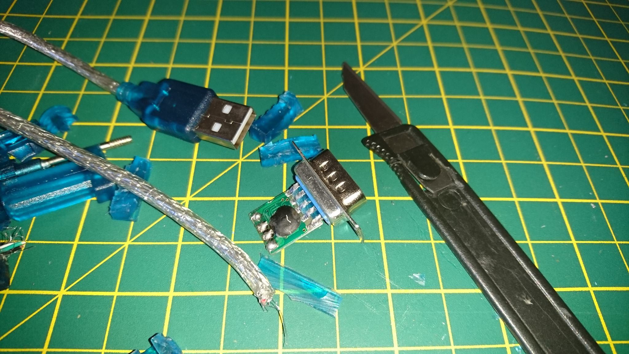
I grabbed my existing USB-to-serial cable and an unterminated Honda cable and, armed with a soldering iron and a scalpel, got to work.
Entombed inside the DB9 end of the cable is a 1cm2 PCB. And I really do mean entombed - the entire board and connections had been put in a mould which had then been filled with soft translucent plastic.
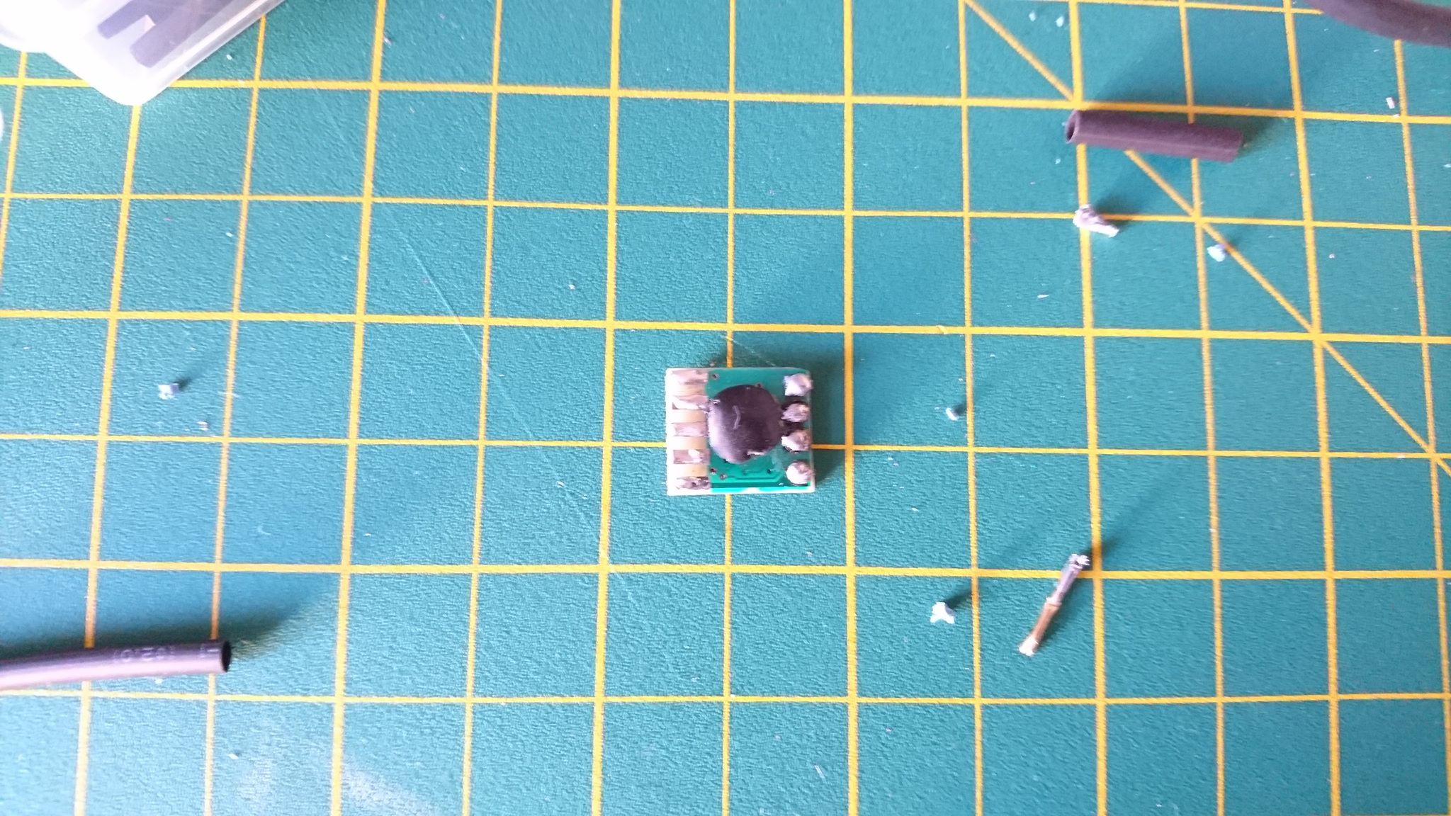
It took me a good hour or so of hacking away with the scalpel to free the board from its rubbery tomb. I also had to cut off the DB9 connector as I didn’t have any desoldering tools good enough to do the job. This is what it looked like when I was done.
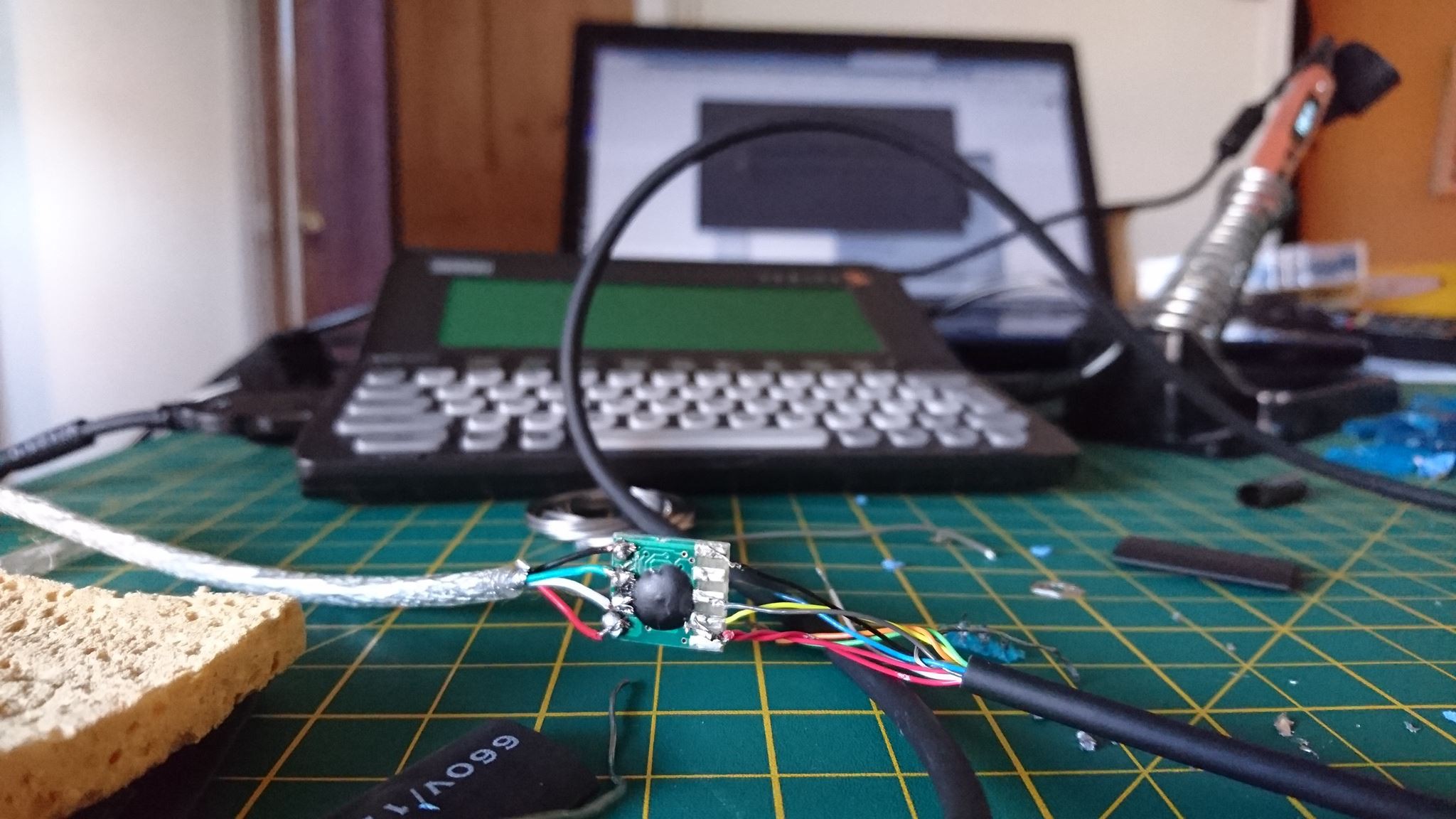
I reused the now unterminated USB cable, slipping some heatshrink onto the cable for later before soldering it to the board. I then soldered an unterminated Honda cable to the serial connectors on the board, again with heatshrink already on the cable. Here's the table with the cable's colour coding and the RS-232 pins they correspond with. (Note that the colours have changed over the years, but these colours worked with the cable I got from eBay.)
DB9
Honda cable colours
Honda pins
RS232
Description
Shield
GND
GND
Shield
1
-
nc
DCD
Data carrier detect
2
Yellow
4 (TX)
RD
received data
3
Grey
8 (RX)
TD
transmitted data
4
Green
5 (DSR)
DTR
data terminal ready
5
Black
15 (SG)
SG
Signal ground
6
Orange
3 (DTR)
DSR
data set ready
7
Red/White
7 (CTS)
RTS
request to send (= DTE ready)
8
Pink
2 (RTS)
CTS
clear to send (= DCE ready)
9
Blue
6 (RI)
RI
Ring indicator
On my first attempt I had soldered the USB’s D- and D+ wires around the wrong way, so I quickly swapped those over. Once I’d fixed that, I crossed my fingers that I hadn’t damaged the board or my PC.
Luckily, I hadn’t. It worked perfectly.
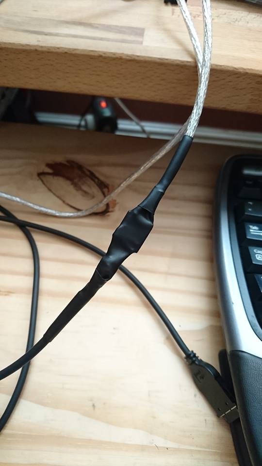
Once that was done I tidied up my soldering, put the large piece of heatshrink in place and aimed a hairdryer at it. I then moved the two smaller pieces of heatshrink and did the same.
I now have a 2m USB to Honda cable that will work on the Series 3c, 3mx and Siena, plus the Series 5 and 5mx, all for about £11.
If I did it again, I would probably find a USB plug enclosure that the CH340 board could fit inside. There is a risk of damage to the solder joints and the PCB and fitting the board inside a small box would fix that. Also, I’d really like to find a supplier who will sell me CH340 boards that don’t require me to hack away at a load of blue plastic.
Oh, and I did work out how to get MASM working, but more on that another time.
I can't believe it's been two months since I last posted here. Much has happened on this project and, although I don't have time to write in detail about these things now, I wanted to give you a brief overview. Warning: Expect Exclamation Marks.
---------- more ----------
A Co-Conspirator Has Been Found!
Karl happened to be working on a Psion SSD project at the same time as me and asked me if I wanted to collaborate. I was apprehensive at first - us techies can be quite possessive of our projects at times - but it's been working brilliantly. We're approaching the SSD challenge from two different angles, which has actually helped in analysing the SIBO platform. So if I refer to "we" rather than "I", you know I'm talking about Karl and me.
SIBO Serial Protocol Cracked!
I've finally managed to get a version of my SIBO-SP decoder released on GitHub. You'll need a copy of PulseView and the sigrok libraries to use them. I'll go into more detail about it in a later post, but I will say thank you to Karl for pointing out that the SIBO-SP data payload is sent LSB first instead of the usual MSB. This is implied in the HDK but not actually explained. Once I'd reversed the bits, suddenly things started to fall into place.
This is so important, as it makes writing libraries and interfacing with an SD card so much easier. The ROM and Flash SSDs, however, use a different format that Karl is in the process of cracking.
New Software!
Karl and I have been talking about writing new software for the SIBO platform, especially RPG, platform and text adventure games. We're putting together a Trello board of ideas. We welcome suggestions, but not too many - we've got plenty to keep us occupied right now!
I got a 3mx!
I found an upgrade. It was dirt cheap. You are allowed to be jealous.
This basically means I have been able to use my old "production" 3c as my main test device. I'll still be using the 3a to check compatibility and also because it has the old-style SIBO serial port.
I got an MC-400!
Possibly the best laptop in the world, and yet is the most useless given that it's practically impossible to get software for it. But I like the idea of trying to get modern software and SSDs running on it, maybe even running a newer version of EPOC16 on it. I'll do a full teardown and review at some point in the future, but for now my focus is the Series 3 range.
There's a lot more to cover, but all in good time. For now, just know that if you've got an old SIBO machine, chances are we're going to be building something that's very 21st century for you.
It's been a relatively fruitful month with this project. After struggling to work out why I was getting some weird signals being measured by my logic analyser (word to the wise: don't forget to connect GND), I managed to get some relatively meaningful waveforms, meaning I could properly start to write a sigrok decoder.
---------- more ----------
Writing a decoder was a slight challenge as I had never touched Python before, but I was able to get something working in about 24 hours!
TheThese screenshots were taken a couple of weeks ago. Since then, I've managed to add some more features to the decoder. I'm not going to lie, the code isn't the prettiest, but it does work. I'll be uploading it to GitHub once I've tidied up the code and added a few more features, along with some of the samples. Feel free to have a play!
The big issue I'm having with this part of the project, though, is not being able to tell which device is talking at any one time. This wouldn't be a problem if the SIBO HDK had the full details of how a SIBO machine talks to an SSD, but unfortunately it only has details of the main SIBO Serial Protocol. While this is immensely helpful, I know that I'm missing a fair amount of information.
One suggestion was to add a resistor at the SSD end of the DATA line and use an oscilloscope to measure the slight voltage drop on anything transmitted by the SSD. Unfortunately I don't (yet) own a scope and I don't think my £4 logic analyser will read analogue signals.
Last week I came across a second way of detecting traffic direction in the SIBO HDK, something I'd missed in previous readings. Pin 59 on the ASIC4 is called SDIR, which goes high when it's sending data. However, my SMD soldering skills aren't brilliant and I think I managed to bork at least one SSD trying to do this. These SSDs will not have died in vain, though, as I will explain later.
Finally, there's the man-in-the-middle option. I now own an Altera MAX II board that I think I could use to forward traffic both ways by detecting when the data line is pulled low at either side, then mirror the traffic on to separate pins. This question on StackOverflow gives an explanation of how this might be done based on some assumptions. However, as I've said before, my VHDL knowledge is non-existent. I'm going to be trying to read up on it as much as possible in the next week to see if I can at least bodge something based on the script in that link.
Even if none of the above work, there is a chance that I might be able to work out what's going on. The ELKS Project was in part an attempt to get Linux running on SIBO machines. Deep in the code there is a very basic SSD driver written in 8086 assembly. This could help massively with writing the code for the eventual Last Psion module. Another option is to rip a copy of the ROM from a SIBO machine, find the driver and disassemble it.
All these options sound plausible, but they're all just out of reach for me at the moment. I still have much to learn.
Now, the dead SSDs. I'm going to try to use them for parts and analysis. There aren't currently any schematics of SSDs available, so I'm going to try to make a couple.
Also, I think the ASIC4 is probably still alive on at least one of them. I've ordered an SMD breakout PCB and some QuikChip, and I'm going to try to move the ASIC to the board. I'm hoping this is going to make it easier to play around with the ASIC, as long as I don't destroy the chip in the process. I could even try to build an SSD using discrete parts...
Finally, one of the SSD enclosures has been "repurposed" as a breakout unit. I managed to connect the Vcc and Vdd around the wrong way on one SSD, which I'm pretty sure didn't do it any favours. The breakout unit will hopefully make sure this doesn't happen again, as well as make it easier for me to connect wires to the port's pins.
Another thing I've discovered is that SIBO talks to Flash and RAM SSDs differently. Add to that the fact that some early SSDs use the ASIC5 rather than the ASIC4, plus that there are two types of Flash SSD, and you've actually got quite a variety of SSD types. I'm waiting for a couple of RAM SSDs to arrive in the post (I don't currently own one), at which point I'll tear them down and hope at least one has an ASIC4. After all, an ASIC4 RAM SSD is what I'm trying to emulate. It's also worth knowing that the ASIC5 doesn't have the SDIR pin that the ASIC4 has, so would make life a little more difficult.
I'm pretty sure that SIBO uses FAT16. I'm also pretty sure that the ASICs are acting as simple block devices. This would mean that all filesystem management is done in SIBO. This seems to be confirmed in the ELKS SSD driver code, which only talks about writing blocks to the ASIC4 rather than writing files or reading directory structures.
I've also finally ordered a 3mx. This should be arriving any day now and will probably become my "production" device. I will still be using the 3c as the target machine for this project. My plan is, of course, for this to work with any SIBO machine that can read an SSD. In that vein, I now own a Workabout MX with a half-working LCD - about half the horizontal lines are dead. Any suggestions on how to repair it, or places I can get a replacement screen, will be gratefully received.
Part of this month has also been spent getting in touch with a lot of people who used to be involved with the Psion world. I do plan on writing something about that in the future, but for now just know that it's been really exciting to talk to these people who were so influential in the Psion world in the 90s.
Finally, I am putting out a scrounging request. If anyone has any old Psion equipment they would be happy to donate to the project, please get in touch. I don't mind if it damaged or even dead, I will take it off your hands. Also, if anyone has any old Psion documentation then please let me know. I've managed to find the HDK and a lot of the SDK as PDFs on the Internet, but I know I'm missing a few documents.
Thanks for reading. I will try to write some more in the next week or so, as well as release the source code for the Sigrok decoder.
I now have everything I need to get started on revealing the secrets of the Psion SSD Port. So, here's what I've been up to this morning.
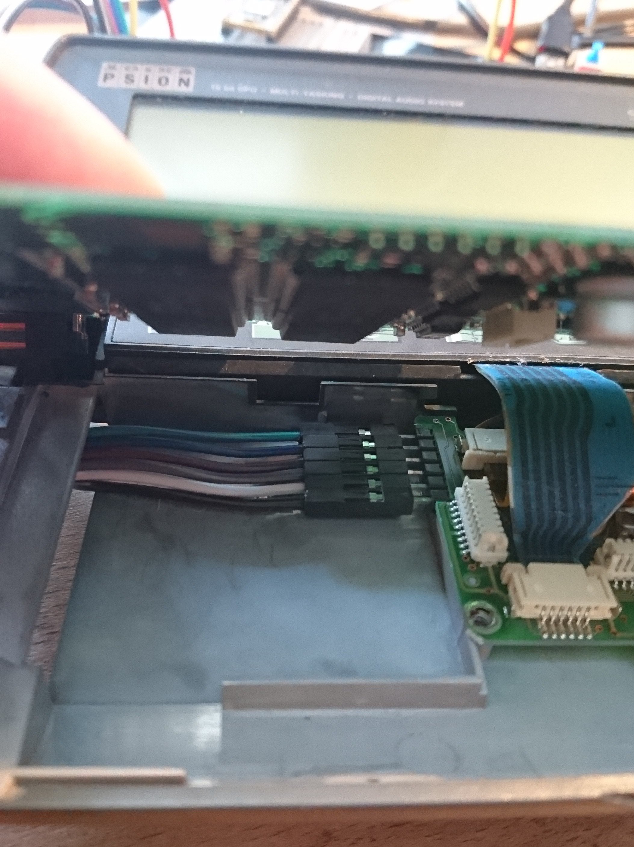
Rather than pull apart my "production" 3c, I've decided to get to work on a slightly broken 3a. I don't like the idea of doing something dumb thanks to my inexperience and blowing up my 3c. The 3a's battery compartment is in a pretty bad way, but it powers on quite happily with a Series 3 external PSU. So, I pulled it apart and got to work.
---------- more ----------
For some reason, this 3a smells really strongly of some spice or other, possibly cumin. It's not pleasant and the unit could really do with a bath in alcohol.
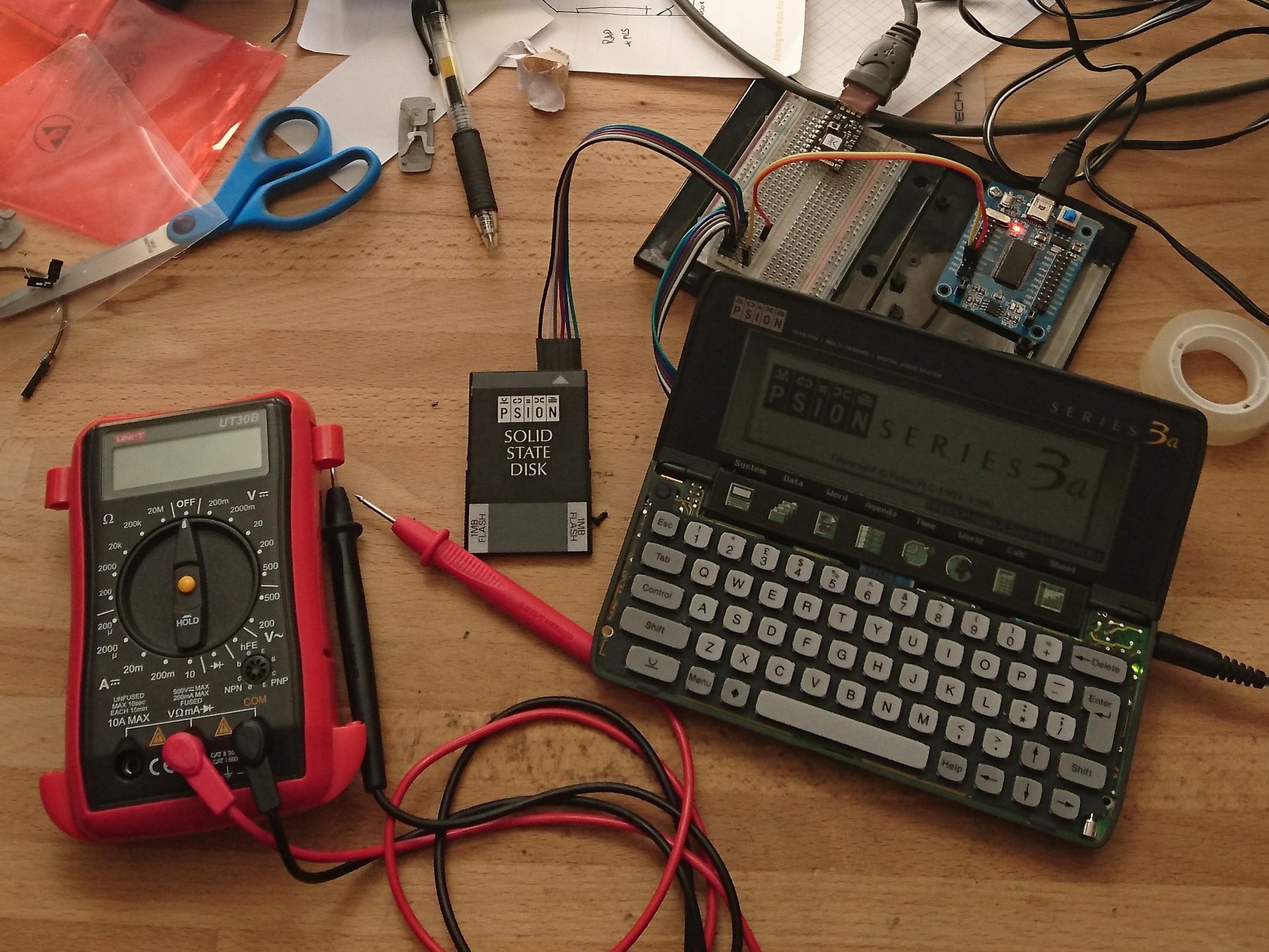
I removed the door for Port A and directly attached six jumper leads to the six pins of Port A. The other ends of the leads were plugged into a solderless breadboard. I then ran a further six jumper leads from the breadboard to my SSD. Keeping my fingers crossed that I hadn't miswired anything (it's currently my only SSD) I powered up the 3a and... it still worked!
My next step was to find out what each pin did. I had already found the SSD pinout using this post from comp.sys.psion.misc, so I used that as basis and used my multimeter to test the voltages on pins 3 to 5. So, here's the updated pinout, using the post on comp.sys.psion.misc as a basis.
Pin
Name
When the 3a is on
When the 3a is off
1
CLK (input to SSD only)
Clock (+5V)
0V
2
GND
GND
GND
3
Vbackup
+3.75V DC
+3.75V DC
4
Vpp (for Flash programming)
+15.75V DC
+9V DC
5
Vcc
+5V DC
0V
6
DATA (bidirectional)
Data (+5V)
0V
Interestingly, the Vpp voltage drop isn't instantaneous, taking just under 10 seconds to drop from 15V to 9V.
So, I have a few questions:
What's the point of Vbackup?
Why does Vbackup stay live when the unit is turned on?
Why does Vpp drop to 9V when the unit is off? Why doesn't it go off completely?
Is there a reason Vpp takes time to drop, or is it just a capacitor taking time to discharge?
UPDATE: I now realise that Vbackup is there to maintain power to RAM SSDs so they don't have to rely on their own internal CR1620 batteries when inside the Psion. This answers questions 1 and 2 - that power is needed even if the Psion is turned off. My guess is that RAM SSDs have Vpp disconnected, Flash SSDs have Vbackup disconnected, and ROM SSDs have both disconnected. It is also worth noting that Vbackup and Vpp are live even if there is no SSD connected and the Psion is off, albeit with Vpp running at 9V. This might prove useful in the future.
I felt it was now time to connect up my USB logic analyser and see if I could use PulseView to see the SIBO Serial Protocol at work. (The other device on the breadboard is an Espruino Pico, which I was using to generate signals to make sure the logic analyser was working.)
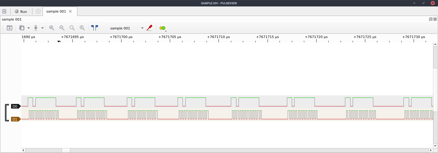
After trying various settings and finally setting the sample rate to 24 MHz, I managed to capture a conversation between the Series 3a and SSD.
The top line is DATA and the bottom is CLK.
PulseView and its backend library sigrok have the ability to do some analysis on the signals they capture. There are plugins for all sorts of protocols, such as I2C, AC '97, SPI. This made me wonder how difficult it would be to write my own plugin for the SIBO Serial Protocol. After a quick look on Google, I found this:
So I think my next step is to see if I can write a protocol decoder for SIBO using the HDK document as a basis. It will help me to understand the protocol better for when I finally get around to building the first SSD prototype.
It’s been a few weeks since my last update on this project. This is partly because I’ve been waiting for a couple of bits to arrive, specifically a logic analyser based on the CY7C68013A and an Altera MAX II EPM240 board. But to be honest, the delay is mostly because I’ve realised how much I need to learn. I mean, I kind of knew that I needed to learn a lot, but I didn’t actually realise how little I already knew. Trust me, folks, Dunning-Kruger is very real and has smacked me in the face with its pointy inverted curve. Again.
---------- more ----------
So, I’ve been learning. One of my first ports of call was Udemy. I’ve got a collection of courses building in my Wishlist, including ones on C, ARM assembly, VHDL and even one on using Blender for 3D printing. But I’ve started the ball rolling with a Crash Course on Electronics and PCB Design by the fantastic André LaMothe. So far the course has been recapping things I learned back in school 25 years ago in Physics and Design Technology lessons, so much of it is familiar to me. But I’m missing a lot of practical knowledge, not to mention having forgotten all the important formulae for working with electricity and electronics. And I know that in a few lessons time I’ll heading into completely new territory. This course is almost 90 hours long and I got it on offer for £10.99. It’s worth much more than that.
I’ve also been trawling YouTube for related videos. I’ve watched a lot of videos on hacking retro hardware, including a batch of videos with someone repairing a lot of Sinclair ZX Spectrums. I’m yet to find any videos of people modifying any Psion kit (he says, trying to drag the narrative back to the project in hand), but maybe I haven’t been looking hard enough. Of course, I’ve watched a lot of the Ben Heck Show, but I guess that’s pretty obligatory.
Otherwise, I’ve been scouring the internet for long-abandoned websites dedicated to Psion kit. It’s been slow going, but I’ve found one or two gems. Of course, if you have any information then please let me know!
Now that the logic analyser and CPLD have arrived and I’ve installed a lot of development software, my next task for this project is to build a breakout board so that I can look at the traffic between the Series 3c and my Psion Flash SSD.
I think I’m going to need to get a stock of old Psion SSDs, both working and dead, because I don’t want to fry my only SSD (which has actual written work on it). If anyone knows anyone with a pile of them going spare, do get in touch. Actually, I’ll take on any old Psion kit, alive or dead. I’m pretty sure I’m going to damage some kit somewhere along the line, especially given my rookie status. Having spares would be invaluable.
Tell any potential donors that it’s for the good of worldwide technological development.
Right, back to the course. Only another 84 hours to go...
When I started thinking about this project, I knew there was going to be quite a steep learning curve. Picking up JavaScript after a long absence, trying to wrap my head around C after trying (and failing) to do so about 20 years ago, learning more about electronics than just holding a soldering iron the right way around.
What I wasn’t expecting to learn was how to design a microchip.
---------- more ----------
As I said in my last log, I am worried that a regular ARM microcontroller won’t be fast enough to handle the 3.84 MHz clock speed of the data coming from the Psion Series 3c. It’s something I hadn’t considered at the beginning, as I assumed that processors had come on enough in the 27 years since the original Series 3 was released that they would be able to handle the speed.
Fortunately, a few very kind people have already sent me messages with ideas on how to tackle this.
On comp.sys.psion.misc (via Google Groups), Theo gave me some food for thought:
The protocol is rather interesting. I think doing it in a CPLD (basic FPGA) would probably be most flexible, but I can understand that's a place you don't want to go. Also, you need to a device with 5V capability, which is quite rare nowadays.
It sounds like the tricky bit is dealing with the up-to-5MHz input signal. I wonder whether you could take a couple of 12-bit shift registers. One is an input, which latches data coming out of the ASIC. The other is an output, which you enable to send data to the ASIC. With a little bit of control logic to handle synchronisation and latching, it essentially reduces your 5MHz one-bit problem to a 400kHz parallel-word problem, which is a lot easier to deal with in software.
Depending what you feel comfortable with, you could have a couple of shift register chips in TTL logic, and then wrap up the control logic in another programmable logic device (PAL, GAL, CPLD, whatever you prefer). Or maybe it's simple enough to do in a few TTL logic gates.
Shift registers didn’t even cross my mind when I started, but using them makes sense. What I need to work out is how to control the data going back to the Psion. I think I would need to monitor the incoming IO, checking the first three bits sent from the 3c for a data request command, then get the output shift register to send data back. (Assuming I have understood the way the SIBO Serial Protocol works, that is.)
The thing is, I hadn't heard of FPGAs before a week ago and the first time I'd come across a CPLD was in Theo's message. So, as I'm sure you can see, using programmable logic chips is a completely different paradigm for me. Using them adds more questions to a project that already seems very complicated to me. For example, will I be able to get enough current from the 3c to be able to power both a CPLD or FPGA and a microprocessor? How do I get them to talk to each other? Not only that, how do I go about learning VHDL?
First, though, I need to really understand what’s going on between an SSD and the 3c. At Theo’s suggestion, I have already ordered a CY7C68013A-based logic analyser (under £4 on eBay, shipped from China) so that I can look at the data going back and forth. In an ideal world I would be able to tell which end of the wire is sending data at any given time. I do like Theo’s suggestion on this:
For instance, gimp the power supply so the SSD voltage is slightly lower than the other, or something like that?
That might be the easiest option. I need to build a “break-out” cable anyway, so that I can use an SSD outside the 3c. Perhaps I can connect up a separate 5v supply on a slightly different voltage? Of course, this could be an ideal project for me to get going with programmable logic.
So, I’m currently worrying about which FPGA or CPLD development board to buy. Do I go with Xilinx or Altera? Is one manufacturer’s software better than the other’s? Do I buy one with an in-built JTAG programmer? What size is suitable for this? How much money is this all going to cost me?
Like I said, I wasn’t expecting to have to think about these things when I started. But I’m not going to lie, there’s part of me that’s a little excited. The kid who wanted to build his own computer is finally getting his wish.
Psion were a clever bunch, but like many companies in the early 90s they didn’t really do standards. Although the 3c and 3mx had a proper RS-232 serial port (albeit using a very odd connector), all of the earlier models used a proprietary protocol called the SIBO Serial Protocol. All Series 3 models used SSDs that also communicated using this proprietary protocol.
A significant part of developing this equipment involves working out how to emulate an SSD or Psion peripheral. Luckily, while trawling the Internet for Psion PDFs I found the Psion SIBO Hardware Development Kit. This book gives a breakdown of how to create equipment for the Psion Series 3 and 3a, including the controller chips needed, the Psion serial protocol, and how to write drivers for the Series 3 and 3a.
The controller chips are known as ASICs, or Application Specific Integrated Circuit chips. As far as I can tell, Psion SSDs mainly use the ASIC4, which converts the SIBO Serial Protocol into addresses within the memory range of the SSD’s on-board memory.
The original ASIC4 has two modes. The first is SSD Mode. This makes the ASIC4 compatible with its predecessor the ASIC5. In this storage-only mode, the ASIC4 can use 21 address bits for memory. As far as I know, this is the way the ASIC4 is configured in every SSD.
The second mode that the ASIC4 can use is called the Extended Mode. This increases the addressable range of memory from 21 bits to 28 bits. Also, the ASIC4 Extended Mode also has a sub-mode called Mixed Mode, which tells the Psion that it's talking to a device that consists of both storage and peripherals. Mixed Mode causes the addressable memory to be split exactly in half, with the lower half used for memory-mapped peripherals and the upper for storage. According to the HDK, this storage is typically used as a ROM including software and drivers to control the peripheral. However, it seems that it can also be used as RAM storage or Flash storage.
As you probably already know, the two aims of this project are to give the Psion both better storage and Wi-Fi access. I'm going to ignore the Wi-Fi challenge for the moment and focus on emulating an SSD, specifically an ASIC4 in Extended Mode. Being able to do that will be an achievement in itself, because it means my 3c will have some modern non-volatile storage.
My first challenge is to deal with the SIBO Serial Protocol. To briefly summarise, this uses a 5v half-duplex two-wire system - CLK and DATA. The 3c controls the clock and sends out 12-bit packets (0-11). Bit 0 and Bit 11 are start and end bits. Sometimes Bits 1 and 2 tell the slave device that it's the slave's turn to send data back on Bits 3-10.
Oh, and the 3c's CLK runs at a nominal 3.84 MHz. Not fast, but not slow either.
What I really want to do is emulate an ASIC4. As far as I see it, I don't need to totally recreate the ASIC4. All I want to do is make my 3c think that it’s talking to an ASIC4 in Extended Mode.
I can see three ways of tackling this:
Completely emulate the ASIC4 on Espruino. This is what I really want to do. But would the Espruino platform be fast enough to cope with the 3.84 MHz clock? I'm guessing pure JavaScript would be nowhere near fast enough to handle it, so a driver would need to be written in C.
Use an original ASIC4 chip. They're not too difficult to get hold of (SSDs pop up all the time on eBay), but there is a finite supply. Also, I would need to remove the chip from an SSD, and I'm not quite at that level of soldering skill yet. Finally, I would need to work out how to get Espruino to talk to an ASIC4.
Emulate the ASIC4 in FPGA. This scares me the most. I haven't got a clue about FPGAs. However, I know it would be insanely fast and mean that I wouldn't have to break SSDs. Still, I'd need to work out how to get Espruino to talk to the FPGA.
If I do try to emulate an ASIC4, I don’t have to emulate the entire chip and all its pins. I just need to make the Psion think it’s talking to an ASIC4. What I don’t know, though, is if an ASIC4 can be connected to an SSD port in Mixed Mode and have the Psion recognise it. Or, to be more accurate, if I can make something that pretends to be an ASIC4 in Mixed Mode and have the Psion recognise it.
Once I have this first major stage working, I will look at emulating Extended Mixed Mode so that I can send commands to the Espruino to control the Wi-Fi.
 Alex Brown
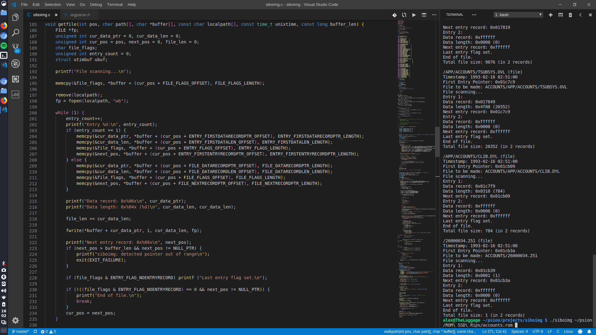

 The decoder:
 Possibly the best laptop in the world, and yet is the most useless given that it's practically impossible to get software for it. But I like the idea of trying to get modern software and SSDs running on it, maybe even running a newer version of EPOC16 on it. I'll do a full teardown and review at some point in the future, but for now my focus is the Series 3 range.
 These screenshots were taken a couple of weeks ago. Since then, I've managed to add some more features to the decoder. I'm not going to lie, the code isn't the prettiest, but it does work. I'll be uploading it to GitHub once I've tidied up the code and added a few more features, along with some of the samples. Feel free to have a play!