Sander van de Bor
-
Uploading sketches to the ATtiny1616
06/02/2019 at 04:35 • 0 commentsThe ATtiny micron-controllers are very popular in the makers community. Only a single capacitor is recommended to stabilize the incoming power and different power sources between 1.8V to 5.5V can be used. The 8MHz internal oscillator will work for most projects and at a cost of about $1 for the DIP version it can be integrated into a project for a fraction of a full blown Arduino UNO.
In order to program micro-controllers programmers are used and offered by the manufactures from these chips. The cost of these programmers start around $50 and can go up to a couple hundreds of dollars. While these programmers are great, and excellent for debugging as well, it is a cost that most makers are not willing to spend. Fortunately the Arduino platform offered a solution where the Arduino UNO can be programmed with a sketch to operate as an SPI programmer. Using the MOSI, MISO, SCK and reset lines allowed uploading sketches through the Arduino UNO to the ATtiny-AVR.
The new ATtiny1616 is a little bit different, and the SPI programmer for the ATtiny-AVR will no longer work. These so called tinyAVR® 1-Series, and similar to the tinyAVR® 0-Series and the megaAVR® 0-series, are using the UPDI 1-wire interface. This new protocol sound very promising since it only requires 1 pin to communicate instead of the 4 pins for SPI and fortunately an Arduino is already there!
El Tangas created a great solution (which can be used on the Arduino UNO) to turn most common Arduino devices into UPDI programmers. The code can be found on Github;
https://github.com/ElTangas/jtag2updi
While a like using the Arduino UNO (I have done all my ATtiny84a projects with the UNO) it is often bulky and requires a lot of wires. An alternative solution is upgrading a AVR JTAG ICE clone with new firmware per following instructions:
https://github.com/ElTangas/jtag2updi/tree/master/tools/avrjtagicev2
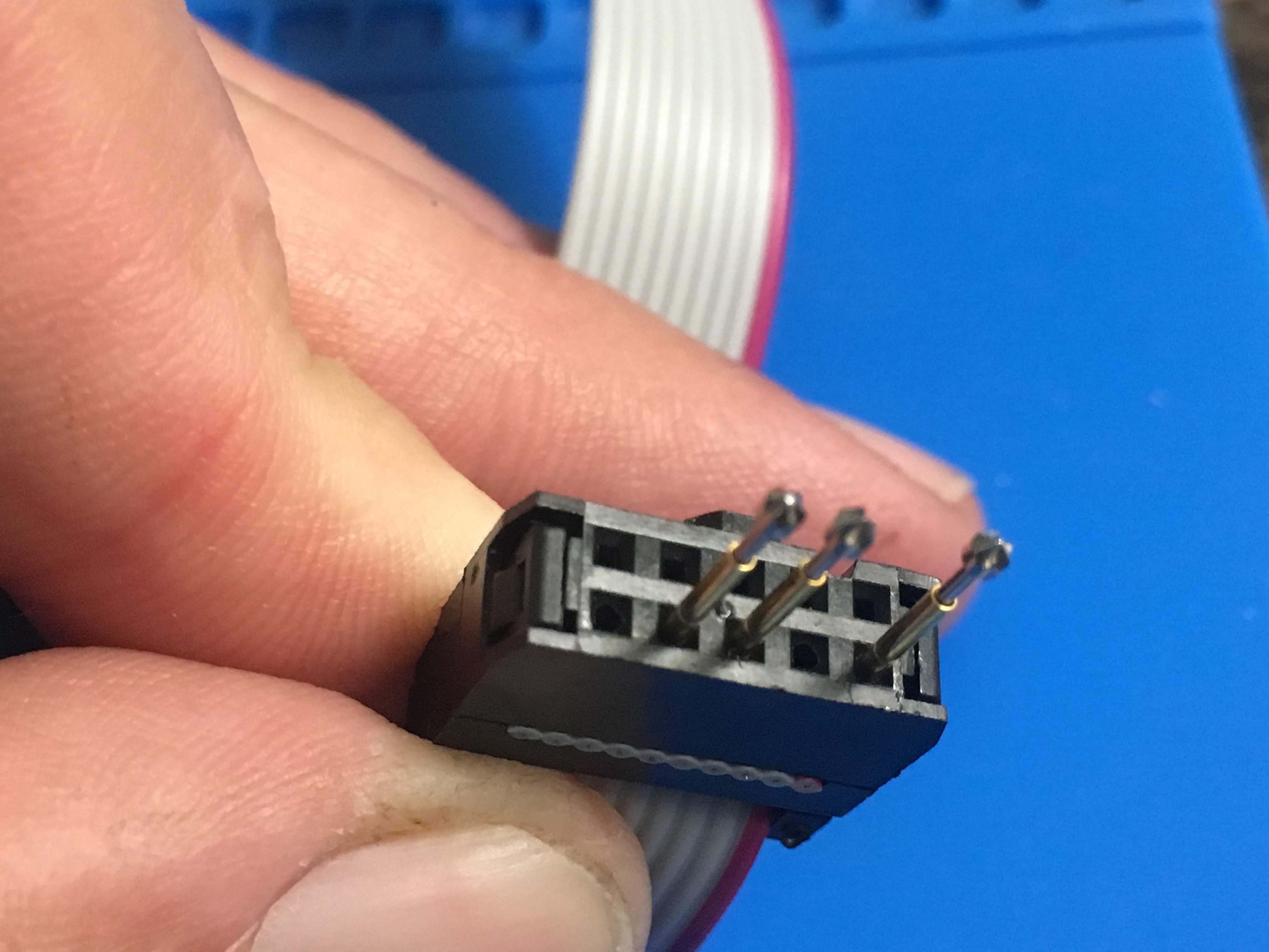
The 10 pin ribbon cable is great, because you can press 1.02 diameter pogo pins into the end.
![]()
It is very similar to the SEGGER pin needle adapters used for programming, but only at a fraction of the cost. While El Tangas shows connecting pin#2 to GND pin#4 for VCC and #6 for UPDI, I decided to use pin #10 for ground instead for the following reasons:
- The DIP break out board for the ATtiny1616 must fit on the bread board, and the VCC and GND need 4 pins spacing between each other, which I get by having VCC on pin #4 and GND on pin #10
- Having the 3 pins separated by an empty pin generates a key so that connecting it to the board will only fit one way (originally the 3 pins were next to each other, so VCC and GND could easily be swapped.
Here is a picture of how this is applied to the board:
![]()
With the pogo pins it is even possible to connect when header pins are applied:
![]()
Next will be the design of the break-out board.
-
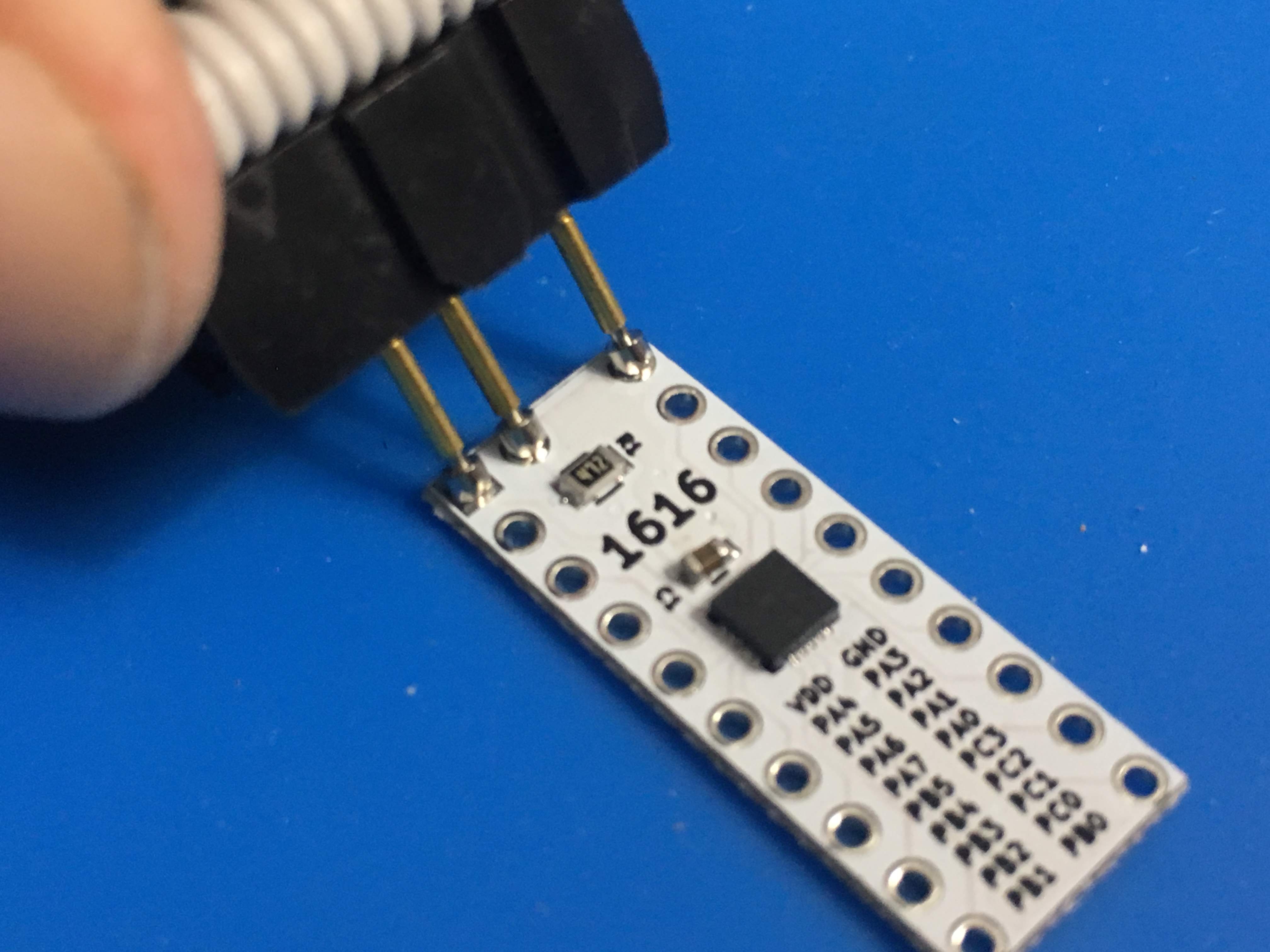
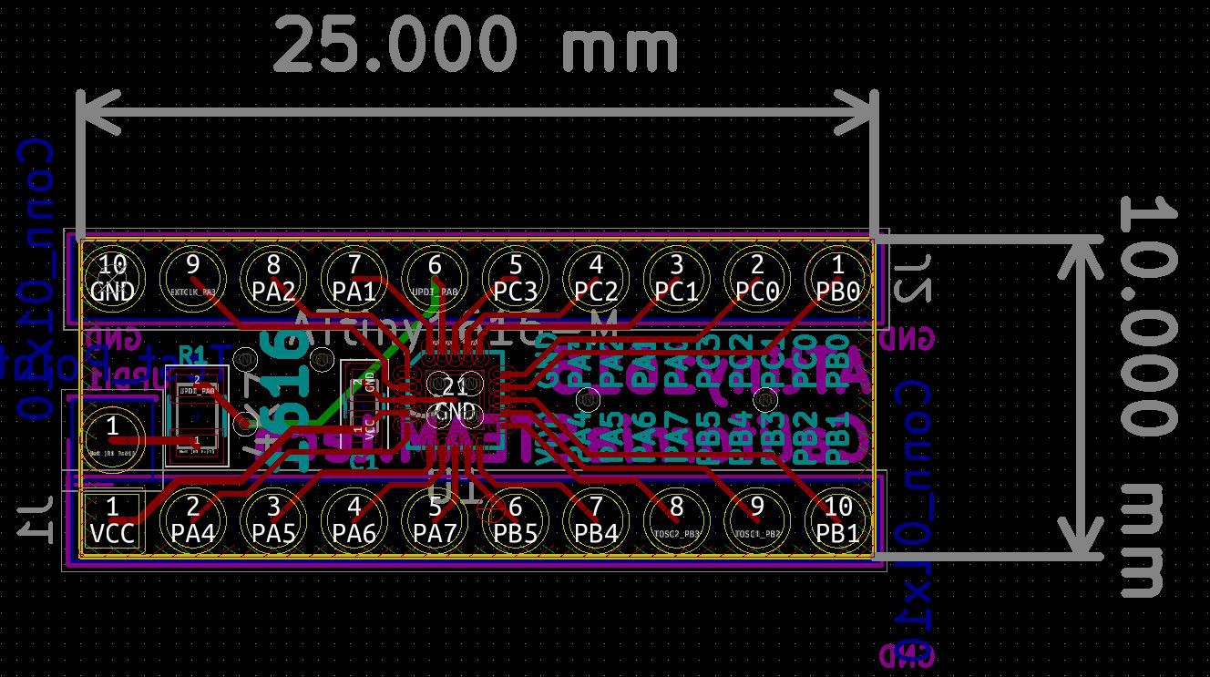
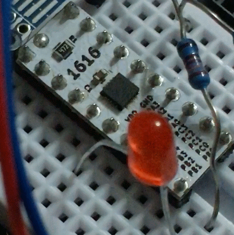
DIP version of ATtiny1616
06/02/2019 at 18:30 • 7 commentsSMD components are getting more popular. They are easy to assemble in production and they get small, very small! Unfortunately with the rise of SMD the through hole version, the Dual In-line Package (DIP), is no longer available for newer micro-controllers and break-out boards are needed to use these on the breadboard.
The ATtiny1616 is available in two packages, the 20-Pin SOIC and the 20-Pin VQFN. For the 20-Pin SOIC there are some break-out boards widely available, for example: https://www.adafruit.com/product/1206
While the SOIC works great, it is relatively large. Instead, the VQFN version is only 3x3MM and allows some additional features which can be added to a custom break-out board for the ATtiny1616.
Since this micro-controller has a build in 20MHz oscillator and will run between 1.8V to 5.5V, there is no need for almost any additional components. A bypass capacitor is recommended between GND and VCC for the microelectronic and a 4.7K Ohm resistor from the programmer to the UPDI pin. The actual pin out position will match the SOIC and see here the results:
![]()
Schematic is available in the files section of this project.
Next step is preparing the Arduino IDE to compile sketches.
-
Preparing Arduino IDE to write sketches for the ATtiny 0- and 1-series
06/04/2019 at 01:36 • 1 commentArduino is a great tool for makers and hobbyists to develop code for tons of different micro-controllers. For the user the code always looks very similar and most code can be compiled for different devices. But in order to make this all happen a lot is happening behind the scenes of Arduino, and a lot of different parties are involved.
Different “translations” are done from the sketch in Arduino to the actual machine code which will be uploaded to the micro-controller. The language the micro-controller is speaking differs for each controller and must be provided by the manufacturer. In this case the ATtiny 0- and 1-series are provided by Microchip and Microchip provides the language in a so-called Device Family Pack (DFP).
When you compile a sketch in Arduino with verbose output turned on (in settings) you will get the location of the compiler and the DFP in the Arduino IDE output window. For example, when you compile a sketch for the Arduino UNO you might see lines like:
C:\Users\username\AppData\Local\Arduino15\packages\arduino\tools\avr-gcc\5.4.0-atmel3.6.1-arduino2\lib\gcc\avr\5.4.0
When you browse to that folder it will show all the different devices that are similar to the micro-controller used on the Arduino UNO (ATMEGA328P), with a complete list shown in the folder device-specs. The files in the device-specs folder are loaded, specific for the micro-controller, to tell the compiler where to find libraries for this device.
Some might notice that the ATtiny1616 is part of the list. Adding the ATtiny 0- and 1-series DFP to Arduino was requested a couple of months ago and they were so kind to make it standard in the latest releases. But just updating the DFP with new packages will not always do the trick. Sometimes new functions are added, and these must be understood by the translator, in this case the compiler.
Arduino is using avr-gcc compiler for the 8-bit microcontrollers. Version 5.4.0 was sufficient for micro-controllers like the ATMEGA328P and the ATtiny series like the ATtiny85 and ATtiny84a. Unfortunately, this compiler version had issues with the new DFP for the 0- and 1-series and a newer compiler version is required (and available).
While the DFP is provided by the manufacturer of the chip, the actual Arduino Core is developed by the Arduino team. It is a collection of libraries which are used to translate the language spoken in Arduino to commands or write to registers described in the DFP. For example, we are all familiar with the delay function. On the Arduino UNO the following function is used (all in the background, so you probably did not even know you were calling out functions):
void delay(unsigned long ms)
{
    uint32_t start = micros();

    while (ms > 0) {
        yield();
        while ( ms > 0 && (micros() - start) >= 1000) {
            ms--;
            start += 1000;
        }
    }
}
Unfortunately, this will not work for the new ATtiny 0- and 1-series, a new core is required.
Luckily enough the Arduino team did come out with a new core and compiler when they released the Arduino UNO WIFI REV2. This new device is using the ATMEGA4809, part of the megaAVR 0-Series, and in the same family as the ATtiny 0- and 1-series. You can see the changes by adding the board from the board manager and just compile an empty sketch with the Arduino Uno WiFi Rev2 board selected. You will notice that the avr-gcc version 7.3.0 is used. The Arduino core is different too, for example the function for delay is now as follows:
void delay(unsigned long ms)
{
    uint32_t start_time = micros(), delay_time = 1000*ms;

    /* Calculate future time to return */
    uint32_t return_time = start_time + delay_time;

    /* If return time overflows */
    if(return_time < delay_time){
        /* Wait until micros overflows */
        while(micros() > return_time);
    }

    /* Wait until return time */
    while(micros() < return_time);
}
With the Arduino core, compiler and DFP in place it should be pretty straight forward to make a variant for the ATtiny series.
Next log will be on creating board variants files.
-
Adding a custom board to Arduino, setting up I/O
06/06/2019 at 00:32 • 3 commentsMost of us start off with the Arduino UNO, but after a while you might try out more advanced boards, or boards from other suppliers, and you must add these board to the board manager. You might end up like me with an endless long list of boards. Adafruit boards, ESP32 and ESP8266, ATtinyCore etc.
I will not go into details how these are created, but when you are interested in the process and want to learn more, there is a good description in the wiki section of the Arduino Github page:
https://github.com/arduino/Arduino/wiki/Arduino-IDE-1.5-3rd-party-Hardware-specification
I have done multiple custom boards before. Added the Micronucleus bootloader to SpenceKonde ATTinyCore; created custom M0+ board and my latest was a custom board with an ATSAME54N20A based on the Metro M4 from Adafruit. So adding a custom variant to MegaAvr should be a piece of cake, at least that was what I thought.
Each board in the board manager has a variant file where mainly all Arduino related naming is linked to a pin, timer, output etc. by mainly using macros. At least, it used to be like that. The MegaAvr variant file still contains a lot of macro’s, but some information is actually stored in the flash memory if the micro-controller. Something new to get used to. The files in the variants folder are named different as well and do contain some additional information. All this information is spread over the following file which you can find in the variants folder for the Arduino Uno WiFi Rev2 and Arduino Nano Every:
- pins_arduino.h
- timers.h
- variant.c
To be flat out honest with everybody, I don’t know where the timers.h is used for (something with time tracking, but isn’t that the Real Time Counter (RTC)?), and the variant.c is currently going over my head and need some more time to understand, so for today I will only focus on pin_arduino.h
When you write to a pin number in Arduino, you are actually setting a bit in a so called PORT. Each PORT is a register, and the length of that register is determined by the type of micro-controller you are using. For example the Arduino UNO is 8 bits, so each PORT controls 8 I/O pins. Since the ATMEGA328P, the micro-controller used on the Arduino UNO, has 23 I/O pins it needs at least 3 registers to control all of these. PORTB controlling 8 I/O pins, PORTC 7, and PORTD 8. You are probably wondering what happened to PORTA. I do not know, but I am sure Atmel at that time had a good reason to start at PORTB, probably because it is sharing the same architecture with other (larger) controllers where PORTA was required for additional I/O pins. While most 32 bits micro-controller have more I/O pins, they require less PORTS since each port can control 32 I/O pins. For example the ATSAMD21G18A, used on the M0, has 38 I/O pins, but only 2 PORTS.
So each PORT is identified by an alphabetic letter and each pin with a number, starting at 0, which will result in pin identifications like PB5, PORTB pin number 5 (keep in mind this is the sixth pin). This concept is important to understand when we start working with the pin_arduino.h file.
We will use the pin_arduino.h located in the C:\Users\username\AppData\Local\Arduino15\packages\arduino\hardware\megaavr\1.8.1\variants
The code start as follows:
#ifndef Pins_Arduino_h
#define Pins_Arduino_h

#include <avr/pgmspace.h>
#include "timers.h"

#define NUM_DIGITAL_PINS            22 // (14 on digital headers + 8 on analog headers)
#define NUM_ANALOG_INPUTS           14
#define NUM_RESERVED_PINS           6  // (TOSC1/2, VREF, RESET, DEBUG USART Rx/Tx)
#define NUM_INTERNALLY_USED_PINS    10 // (2 x Chip select + 2 x UART + 4 x IO + LED_BUILTIN + 1 unused pin)
#define NUM_I2C_PINS                2  // (SDA / SCL)
#define NUM_SPI_PINS                3  // (MISO / MOSI / SCK)
#define NUM_TOTAL_FREE_PINS         (NUM_DIGITAL_PINS)
#define NUM_TOTAL_PINS              (NUM_DIGITAL_PINS + NUM_RESERVED_PINS + NUM_INTERNALLY_USED_PINS + NUM_I2C_PINS + NUM_SPI_PINS)
#define ANALOG_INPUT_OFFSET         14
It uses some macros to name some variables which are used throughout the Arduino Core. The NUM_DIGITAL_PINS and NUM_ANALOG_INPUTS are pretty straight forward; it is the number of pins on the board which are used for digital I/O followed by the number of pins used for analog input. This is not much different from previous boards, but some of the other identifiers are new to me, like the NUM_TOTAL_FREE_PINS and ANALOG_INPUT_OFFSET. It is not important at this moment and I will get back to it after I figure it all out.
Let’s go down to line# 118. Here you can find a graphical ASCII representation of the ATMEGA4809 micro-controller with a label for all the pins.
//                     (SCL)(SDA) (7)  (2)                 (R)  (3~) (6~)
//                 PA4  PA3  PA2  PA1  PA0  GND  VDD  UPDI PF6  PF5  PF4  PF3
//
//                  48   47   46   45   44   43   42   41   40   39   38   37
//              + ____ ____ ____ ____ ____ ____ ____ ____ ____ ____ ____ ____ +
//        PA5   1|                                                             |36  PF2
//        PA6   2|                                                             |35  PF1 (TOSC2)
//        PA7   3|                                                             |34  PF0 (TOSC1)
//   (9~) PB0   4|                                                             |33  PE3 (8)
//  (10~) PB1   5|                                                             |32  PE2 (13)
//   (5~) PB2   6|                                                             |31  PE1 (12)
//        PB3   7|                          48pin QFN                          |30  PE0 (11~)
//   (Tx) PB4   8|                                                             |29  GND
//   (Rx) PB5   9|                                                             |28  AVDD
//        PC0  10|                                                             |27  PD7 (VREF)
//        PC1  11|                                                             |26  PD6
//        PC2  12|                                                             |25  PD5 (A5)
//               + ____ ____ ____ ____ ____ ____ ____ ____ ____ ____ ____ ____ +
//                  13   14   15   16   17   18   19   20   21   22   23   24
//
//                  PC3  VDD  GND  PC4  PC5  PC6  PC7  PD0  PD1  PD2  PD3  PD4
//                                 (1)  (0)  (4)       (A0) (A1) (A2) (A3) (A4)
The leg number of the pin is closest to the board, for example 4, followed by the pin identification PB0 (PORT B, first pin), and some have a number or description in parentheses, in this case 9~. 9 is the actual pin number on the board, and the number used in Arduino. In Arduino, digitalWrite(9, HIGH) will turn on PB0. The tilde (~) next to the 9 is there to identify that this can be used as an PWM output. PWM requires timers to setup, so I will get back to that later as well.
The ATMEGA4809 has 41 I/O pins, so needs at least 6 PORTS, and looking at the drawing we see that PORTA up to PORTF are used for that.
Underneath the graphical representation of the board there are some arrays created to be stored in Flash memory. The first array, digital_pin_to_port, only list which PORT each pin belongs to. The order of the array is important, because it is in order of the Arduino pin assignment. Like the Arduino UNO (and most Arduino boards), the first 2 pins are using the RX and TX and that are also the first two variables in the array, pin 0 and 1:
const uint8_t PROGMEM digital_pin_to_port[] = {
  PC, // 0 PC5/USART1_Rx
  PC, // 1 PC4/USART1_Tx
The second array, digital_pin_to_bit_position, is showing the location of the pin within the PORT. In our earlier example above, Arduino board pin#0 is on PC5, so the digital_pin_to_bit_position will bePIN5:
const uint8_t PROGMEM digital_pin_to_bit_position[] = {
  PIN5_bp,  // 0 PC5/USART1_Rx
  PIN4_bp,  // 1 PC4/USART1_Tx
Same is done for the digital_pin_to_bit_mask.
The next two arrays are for controlling analog I/O. For now we do not worry about the digital_pin_to_timer, neither the analog_pin_to_channel.
Setting up the ATtiny1616
We are going to use the ATtiny1616 datasheet to configure the I/O PORTS and pins. The full datasheet can be found here:
http://ww1.microchip.com/downloads/en/DeviceDoc/ATtiny3216_ATtiny1616-data-sheet-40001997B.pdf
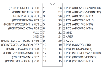
These documents are usually a pain to read through but let me guide you through some of the most important information. Chapter 4 (page 14) shows the pin-out for the SOIC and VQFN version. While the actual legs on both packages do not match, for example leg 2 on the SOIC is PA4 and PA3 on VQFN, that will not matter for writing the software since we will be using PORT and the pin inside that PORT. The ATtiny1616 breakout board contains the VQFN version, but it break-out like the SOIC version, so we will be using that for reference. Here is the ASCII version of the 20-Pin SOIC version
// ATtiny1616 / ARDUINO
//         _____
//  VDD  1|*    |20  GND
//  PA4  2|     |19  PA3
//  PA5  3|     |18  PA2
//  PA6  4|     |17  PA1
//  PA7  5|     |16  PA0
//  PB5  6|     |15  PC3
//  PB4  7|     |14  PC2
//  PB3  8|     |13  PC1
//  PB2  9|     |12  PC0
//  PB1 10|_____|11  PB0
We are going to give all the I/O pins Arduino pin numbers starting at the upper left corner, and going counter clockwise to the upper right corner, which will result in the following.
// ATtiny1616 / ARDUINO
//                   _____
//        VDD      1|*    |20      GND
//  (nSS) PA4  0   2|     |19  16  PA3 (EXTCLK)
//        PA5  1   3|     |18  15  PA2 (MISO)
//  (DAC) PA6  2   4|     |17  14  PA1 (MOSI)
//        PA7  3   5|     |16      PA0 (nRESET/UPDI)
//        PB5  4   6|     |15  13  PC3
//        PB4  5   7|     |14  12  PC2
//(TOSC1) PB3  6   8|     |13  11  PC1
//(TOSC2) PB2  7   9|     |12  10  PC0
//  (SDA) PB1  8  10|_____|11   9  PB0 (SCL)
You will notice that PA0 did not get an Arduino Pin number, mainly because this pin is used to program the chip using UDPI and cannot be used for I/O. All this information is used to complete the digital_pin_to_port, digital_pin_to_bit_position and digital_pin_to_bit_mask as follows:
const uint8_t PROGMEM digital_pin_to_port[] = {
    // Left side, top to bottom
    PA, // 0  PA4
    PA, // 1  PA5
    PA, // 2  PA6
    PA, // 3  PA7
    PB, // 4  PB5
    PB, // 5  PB4
    PB, // 6  PB3
    PB, // 7  PB2
    PB, // 8  PB1
    // Right side, bottom to top
    PB, // 9  PB0
    PC, // 10 PC0
    PC, // 11 PC1
    PC, // 12 PC2
    PC, // 13 PC3
    PA, // 15 PA1
    PA, // 16 PA2
    PA  // 17 PA3
};

/* Use this for accessing PINnCTRL register */
const uint8_t PROGMEM digital_pin_to_bit_position[] = {
    // Left side, top to bottom
    PIN4_bp, // 0  PA4
    PIN5_bp, // 1  PA5
    PIN6_bp, // 2  PA6
    PIN7_bp, // 3  PA7
    PIN5_bp, // 4  PB5
    PIN4_bp, // 5  PB4
    PIN3_bp, // 6  PB3
    PIN2_bp, // 7  PB2
    PIN1_bp, // 8  PB1
    // Right side, bottom to top
    PIN0_bp, // 9  PB0
    PIN0_bp, // 10 PC0
    PIN1_bp, // 11 PC1
    PIN2_bp, // 12 PC2
    PIN3_bp, // 13 PC3
    PIN1_bp, // 15 PA1
    PIN2_bp, // 16 PA2
    PIN3_bp  // 17 PA3
};

/* Use this for accessing PINnCTRL register */
const uint8_t PROGMEM digital_pin_to_bit_mask[] = {
    // Left side, top to bottom
    PIN4_bm, // 0  PA4
    PIN5_bm, // 1  PA5
    PIN6_bm, // 2  PA6
    PIN7_bm, // 3  PA7
    PIN5_bm, // 4  PB5
    PIN4_bm, // 5  PB4
    PIN3_bm, // 6  PB3
    PIN2_bm, // 7  PB2
    PIN1_bm, // 8  PB1
    // Right side, bottom to top
    PIN0_bm, // 9  PB0
    PIN0_bm, // 10 PC0
    PIN1_bm, // 11 PC1
    PIN2_bm, // 12 PC2
    PIN3_bm, // 13 PC3
    PIN1_bm, // 15 PA1
    PIN2_bm, // 16 PA2
    PIN3_bm  // 17 PA3
};
That is all for the digital I/O. I made some additional changes to some of the libraries and variant.c file before I was able to compile but will share those in the next logs. All current development of the code can be found on Github:
https://github.com/SpenceKonde/megaTinyCore
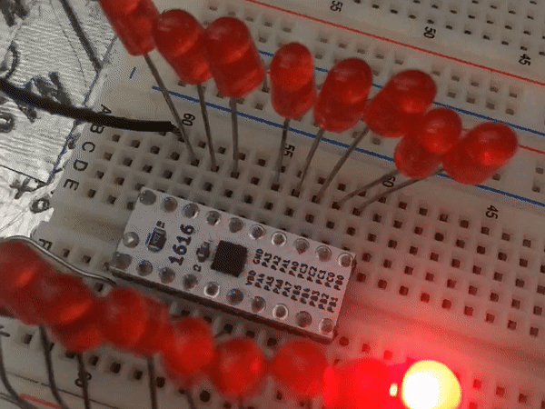
Testing the digital I/O set in Arduino can be done with a simple program and some LED’s on the output pins.
byte numPins=17;

void setup() {
  for (int i = 0; i <= numPins; i++) {
    pinMode(i, OUTPUT);
    digitalWrite(i, HIGH);
  }
}

void loop() {
  for (int i = 0; i <= numPins; i++) {
      digitalWrite(i, LOW);
      delay(50);
      digitalWrite(i, HIGH);
  }
}
Results in:
![]()
PORTMUX is next!
-
PORTMUX on the 0- and 1- series explained
06/08/2019 at 03:34 • 2 commentsGrocery shopping was easy where I grew up. The store was small, and the options limited. Need milk, you grab a carton, tea did not have thousands of different flavors and beer was just a Pilsener. Today is different and you can spend hours in the store since there are too many options, just like the peripherals on these new micro-controllers.
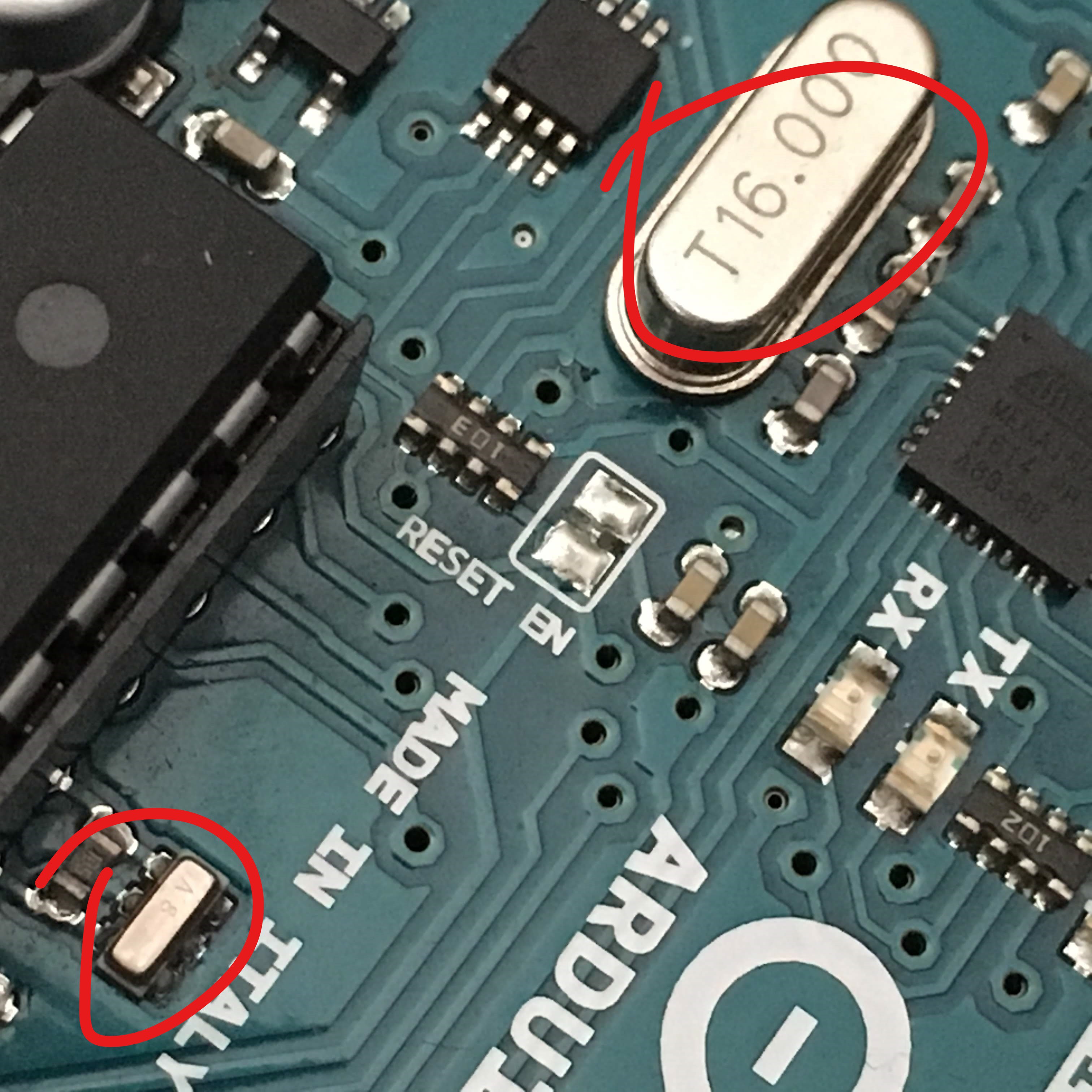
The ATMEGA328P used in the Arduino UNO is pretty good controller and suit most of my projects. It has some nice peripherals to other devices as you can see in the picture below:
You can create an SPI connection with pins PB2 to PB5 (SS, MOSI, MISO and SCK). Have a “serial” (UART) connection with PD0 (RXD) and PD1 (TXD) and create a wire connection with PC4 (SDA) and PC5 (SCL). All the analog inputs are on PC0 (ADCx) up to PC5, but there is also a conflict since PC4 and PC5 were used for wire already. So, when you use wire, you basically only have ADC0 up ADC3 left for analog inputs since the others (ADC4 and ADC5) are used.
The more advanced 32 bits micro-controllers like the SAMD21G18A, used on the Arduino M0, has even more peripherals per pin. A pin could have up to 8 different peripherals and a conflict between pins is more common. Fortunately, unlike the ATMEGA328P, you can move certain peripherals around between certain pins when pins are used for something else. For example, with the issue above where we want to use all the analog input pins, there will be an option on more advanced micro-controllers to move the SDA and SCL pins to a different pins of even a PORT. This is all described in the PORT Function Multiplexing table and called PORTMUX. The ATMEGA4809 supports PORTMUX and so does the ATtiny1616. I will skip the more advanced micro-controllers and go straight to the ATtiny1616 since that has the easiest PORTMUX table I have worked with so far.
The PORTMUX table can be found on page#16 (chapter 5) of the ATtiny1616 datasheet:
http://ww1.microchip.com/downloads/en/DeviceDoc/ATtiny3216_ATtiny1616-data-sheet-40001997B.pdf
For our ATtiny1616 break-out board we want at least all the 3 serial communication options (USART, SPI and TWI) and as many PWM (TCA) and analog input pins (ADC). The ATtiny1616 even supports 1 analog output (DAC)! The PORTMUX table mentioned above is added to the pins_arduino.h variant file for reference as wel (see: https://github.com/SpenceKonde/megaTinyCore/blob/master/megaavr/variants/csat1616/pins_arduino.h).
You will notice that the columns USART0, SPI0, TWI0, TCA0, TCBn and CCL have the same description on multiple pins. For example, MOSI is shown behind PA1 and PC1. That does not mean the ATtiny1616 support two individual SPI peripherals, you must pick one of the two. You might also notice that one is in typewriter font which means that it is the alternative pin location for that peripheral.
Based on this table I was able to update the ASCII board lay-out from my previous log:
                          _____
                  VDD   1|*    |20  GND
 (nSS)  (AIN4) PA4  0~  2|     |19  16~ PA3 (AIN3)(EXTCLK)
        (AIN5) PA5  1~  3|     |18  15  PA2 (AIN2)(MISO)
 (DAC)  (AIN6) PA6  2   4|     |17  14  PA1 (AIN1)(MOSI)
        (AIN7) PA7  3   5|     |16      PA0 (nRESET/UPDI)
        (AIN8) PB5  4   6|     |15  13  PC3
        (AIN9) PB4  5   7|     |14  12  PC2
 (RXD) (TOSC1) PB3  6   8|     |13  11  PC1
 (TXD) (TOSC2) PB2  7~  9|     |12  10  PC0
 (SDA) (AIN10) PB1  8~ 10|_____|11   9~ PB0 (AIN11)(SCL)
For now I just picked all the standard locations, but I might move the SPI pins to PC0 to PC3 or use the ADC1 in the future since those pin in PORTC are available and not really used for something else besides regular I/O. Using alternative pin locations requires register changes which I will describe in another log. The following changes are made to the pins_arduino.h with the following settings for all Serial communication:
#define SPI_MUX              (PORTMUX_SPI0_DEFAULT_gc)
#define PIN_SPI_MISO    (15)
#define PIN_SPI_SCK        (16)
#define PIN_SPI_MOSI    (14)
#define PIN_SPI_SS        (0)

#define MUX_SPI            (SPI_MUX)
#define SPI_INTERFACES_COUNT    1

static const uint8_t SS   = PIN_SPI_SS;
static const uint8_t MOSI = PIN_SPI_MOSI;
static const uint8_t MISO = PIN_SPI_MISO;
static const uint8_t SCK  = PIN_SPI_SCK;

#define PIN_WIRE_SDA        (8)
#define PIN_WIRE_SCL        (9)

#define TWI_MUX         (PORTMUX_TWI0_DEFAULT_gc)

static const uint8_t SDA = PIN_WIRE_SDA;
static const uint8_t SCL = PIN_WIRE_SCL;

// Mapped to HWSERIAL0 in Serial library
#define HWSERIAL0                 (&USART0)
#define HWSERIAL0_DRE_VECTOR     (USART0_DRE_vect)
#define HWSERIAL0_DRE_VECTOR_NUM (USART0_DRE_vect_num)
#define HWSERIAL0_RXC_VECTOR     (USART0_RXC_vect)
#define HWSERIAL0_MUX             (PORTMUX_USART0_DEFAULT_gc)
#define PIN_WIRE_HWSERIAL0_RX     (6)
#define PIN_WIRE_HWSERIAL0_TX     (7)
The USART communication can be tested with a Serial to USB converter, for example the https://www.adafruit.com/product/3309, but any converter will work. Just connect the RxD pin on the converter to PB2 (TxD) in the ATtiny1616 and make sure they both share the ground. You could power the ATtiny1616 from the 5V connection of the converter as well when you don't have a power supply for your board yet. Here is a simple program written in Arduino to test the connection:
void setup() {
    Serial.begin(115200);
}

void loop() {
  for (int i = 0; i <= 10; i++) {
    Serial.print(i);
    Serial.print(" ... ");
    delay(500);
  }
  Serial.println("Hello World!");
}
Which will result in the following output:
![]()
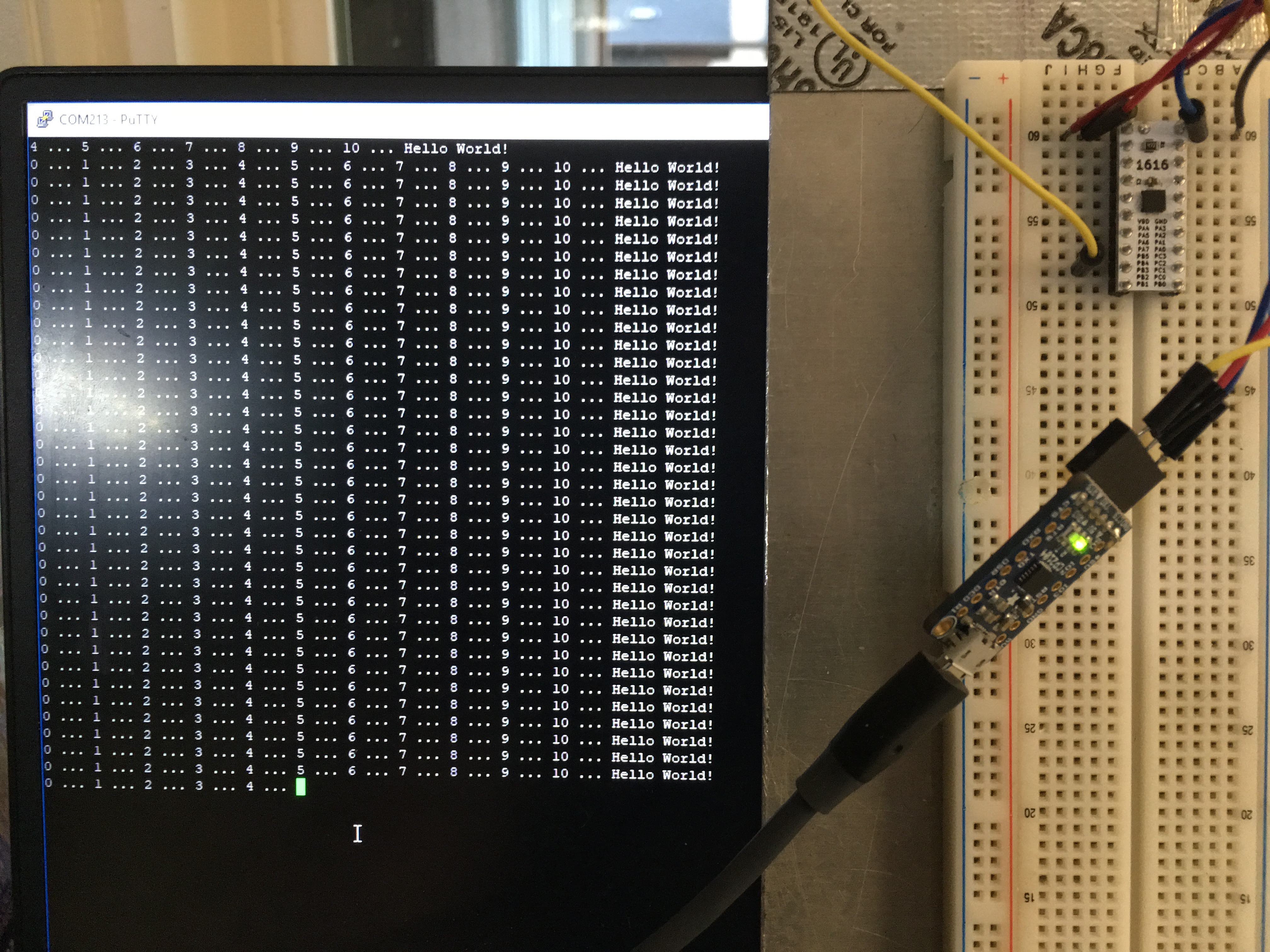
I used the program PuTTY to connect to the serial port since I have the programmer connected in Arduino and I did not want to switch between serial ports to establish a Serial Monitor connection.
Next I will explain the registers a little bit more in details. There is not a lot of documentation on these new chips and I have not found a clear explanation of how these should be programmed (structure wise) but I get a better understanding after reading the datasheet and playing with ATMEL start.
-
New method for writting registers on the 0- and 1-series
06/08/2019 at 05:21 • 0 commentsArduino uses a lot of functions and macros to make it easier for an end-user, with some minor programming and no micro-controller experience, to develop a sketch. Without using these functions, but still using macros, a program for the ATMEGA328P will look like this:
int main(void) {
  DDRB |= (1 << 2);
  while (1) {
    PORTB |= (1 << 2);
    _delay_ms(1000);
    PORTB &= ~(1 << 2);
    _delay_ms(1000);
  }
  return 0;
}
DDRB and PORTB are both macros and are referring to a register on the ATMEGA328P.
This example above sets PB2 as an output and toggles it on and off. Read by someone experienced in C or C++, but with no experience with the AVR, this code will probably not make any sense. What is DDRB, and why do we write a value to PORTB?
DDRB and PORTB are macro’s and converted by the preprocessor to a register address. DDRB is address 0x04 and PORTB is 0x05. See page#100 of the datasheet for more information: http://ww1.microchip.com/downloads/en/DeviceDoc/ATmega48A-PA-88A-PA-168A-PA-328-P-DS-DS40002061A.pdf
But why use macro names that are so hard to understand. Often I hear that a good written code does not need any comments since the variables should be clear to understand.
Here comes the beauty of these new 0- and 1-series micro-controllers where almost every register and every variable going into those registers has a label or name that makes more sense. You can find all of these labels in the C:\Users\username\AppData\Local\Arduino15\packages\arduino\tools\avr-gcc\7.3.0-atmel3.6.1-arduino5\avr\include\avr folder and just compare IOM4809.IO (229KB for ATMEGA4809) vs iom328p.h (20KB for ATMEGA328P). Here is a simple example of the same code above for the ATtiny1616:
int main(void)
{
  PORTB.DIRSET= PIN2_bm;
  While (1) {
      PORTB.OUTSET = PIN2_bm;
      _delay_ms(1000);
      PORTB.OUTCLR = PIN2_bm;
      _delay_ms(1000);
  }
}
It is a little bit easier to read. DIRSET set the direction of PIN2 of PORTB followed by setting and clearing the output with OUTSET and OUTCLR using PIN#2 bitmask.
See this blog for some more information:
http://leoninstruments.blogspot.com/2014/05/xmega-tutorial-ports-04.htmlEverything we do on the micro-controller is done by setting bits in registers. As you can see above you can shift bits in and out or use macros. Macros are not slowing down your code or increasing your compiled code, because the values for the macros replaced in your code by the preprocessor before it will be compiled. These macros are getting very helpful when you work with the registers for peripherals.
The addresses of registers for peripherals can be found in the datasheet for the ATtiny1616 on page#44 (http://ww1.microchip.com/downloads/en/DeviceDoc/ATtiny3216_ATtiny1616-data-sheet-40001997B.pdf)
You will see the base address in the first column and a description in the second. This is just a base address, a lot more registers for these peripherals after this base address could be reserved to store data, for example PORTMUX has a base of 0x0200. Going to page#138 shows the registers following this PORTMUX baseline of 0x0200 and the needed offset. For example, CTRLB has an offset of 0x01, so it has the address of 0x0200 + 0x01 = 0x0201.
In this register you can set the alternative pin locations for SPI0 and USART0. Just shifting in a bit to turn on the first bit will activate USART0 on the alternative pin. Instead if using bit shifts, there are actually macros created for each possible combination, which will result in the following code:
PORTMUX.CTRLB|= PORTMUX_USART0_DEFAULT_gc; // does this -> (0x0200 + 0x01 |= (0x00<<0)I recommend looking at the log of Simon’s project since it has some other great examples of how to use the macros on this new 0- and 1-series AVR’s as well:
https://hackaday.io/project/165439-attiny-0-series-programming-on-the-cheap
-
Timers, use the RTC to blink LED
06/15/2019 at 04:16 • 0 commentsIn our world we use clocks to keep track of time and in the micro-controller world we use timers to count the clock. Clocks used in microcontrollers do not keep track of time!
Timers on the micro-controller can be confusing and could be hard to understand but are so important for the microcontroller to operate. For example, when we like to flash a single LED every 500 millisecond, then we must keep track of time somehow. Almost every micro-controller out there has at least one or two timers, the ATtiny84a had 2, the ATtiny1616 has 4. But a timer will not count (the method to keep track of time) by itself. It needs an input, a source from something that pulses, called a clock. The most common clock is an oscillator and some microcontrollers have some build in. Most of the older controllers uses external oscillators for a better accuracy, for example the Arduino UNO has two:
![]()
Fortunately, the ATtiny has internal oscillators that are sufficient for most project. The internal oscillator for the Attiny84a used to be calibrated for 8MHz, this new ATtiny1616 uses a 16/20 MHz low-power RC oscillator.
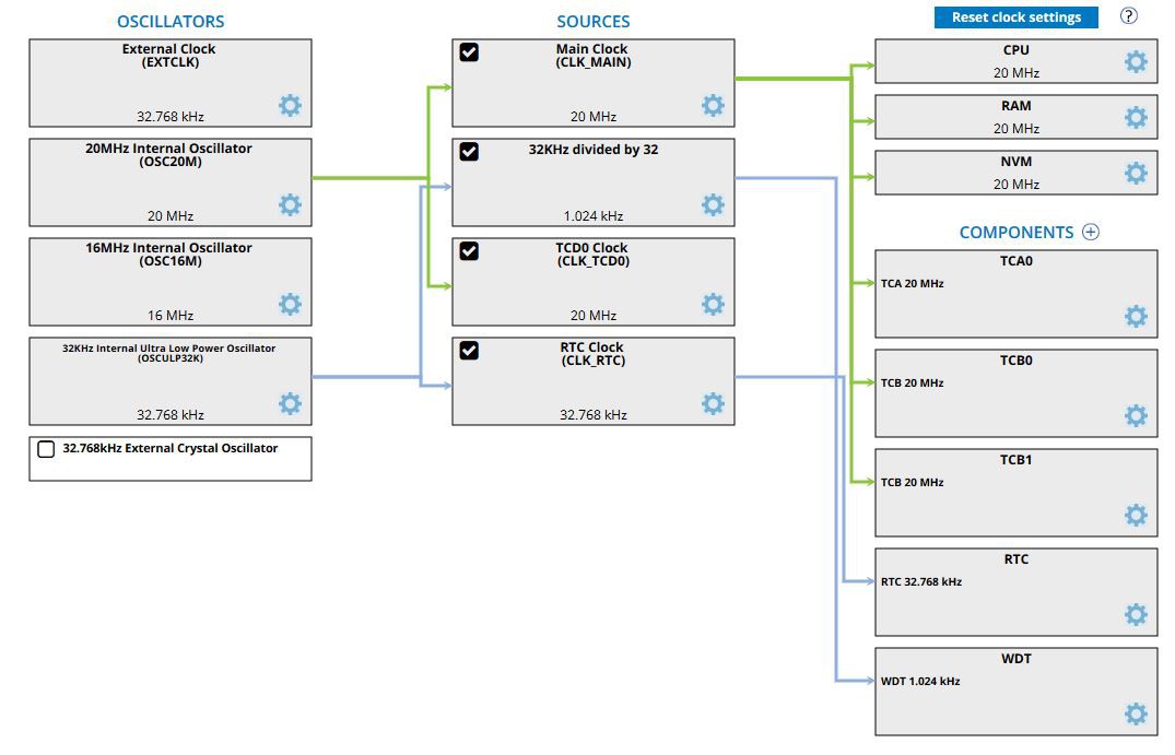
These clocks are used as an input to the timers and currently configured as follows (taken from the Atmel Start application):
![]()
On the left you see the different oscillators, where the 3 options in the middle (20MHz, 16MHz and 32KHz) are internal and the other two external. In the middle are the sources, where the clock can be manipulated before getting used. For example, the Main Clock can be divided by 2 which will result in a 10MHz source for peripherals on the right (and the CPU will run only at half the speed). Running the CPU at a slower speed can help to reduce the power consumption.
Under components you see the actual timers used by the micro-controller, and if you are paying attention you might notice that there are 5 timers listed, not 4 I mentioned above. It gets even more complicated! According to the ATtiny1616 spec sheet there are 4 timers: Timer/Counter Type A (TCA0), Timer/Counter Type B (TCB0 and TCB1), and the fourth Timer/Counter Type D (TCD0). TCD0 is actually listed under sources, probably because it is always active while the other components could be turned off (and they do not appear on the picture above).
The WDT is the Watch Dog Timer. Yes, it is a timer, but cannot be used to execute some code on the ATtiny1616. The WDT can only be used to reset the microcontroller when it gets stuck in some code (an infinite loop).
RTC is the real time counter. It is not a timer, it is a time counter. To be honest that confuses the heck out of me as well. The RTC is actually a great counter which you will appreciate for your low power consumption projects. On the older ATtiny’s the WDT could be used to wake-up the micro-controller, but that is not longer an option on the ATtiny1616; it is done with the RTC.
You can see above that almost all the timers use the 20MHz oscillator. The 20MHz is accurate (±2%), but will use some power to run it. The RTC and WDT are using the 32.768 kHz (note it can be written as 32Khz as well which is 32khz*1024), which is slow and not so accurate (±10% when not calibrated), but the power consumption is very low! It is also a timer which is probably not going to be used by anything else on the Arduino, so it will be available without any interference with other existing code.
In this example I am going to demonstrate how to use RTC to blink an LED, the “hello world” of the Arduino. I will introduce some new instructions which can be used.
We probably all know how to make an LED blink in Arduino, there is even an example in the IDE called blink:
void setup() {
  pinMode(LED_BUILTIN, OUTPUT);
}

void loop() {
  digitalWrite(LED_BUILTIN, HIGH);   // turn the LED on (HIGH is the voltage level)
  delay(1000);                       // wait for a second
  digitalWrite(LED_BUILTIN, LOW);    // turn the LED off by making the voltage LOW
  delay(1000);                       // wait for a second
}
I used to replace the loop with the following code, and it was possible since HIGH and LOW were just a BOOL of 0 or 1, to make it shorter:
digitalWrite(LED_BUILTIN, digitalRead(LED_BUILTIN));   // turn the LED on  or off based on previous state
delay(1000);                       // wait for a second
That no longer works with the new core since it has some more options besides HIGH and LOW, CHANGE can be used to toggle the output, resulting in:
digitalWrite(LED_BUILTIN, CHANGE);   // toggle the LED
delay(1000);                         // wait for a second
Running this code will result, as expected, with an LED to turn on and off using PIN#4.
![]()
Using delay is convenient, but it has a big disadvantage, the CPU cannot do something else at that moment. It is basically checking (for thousands of cycles) if it reached to set delay time. So the CPU is wasting energy on nothing at that moment.
There are tons of examples out there that use millis, but there is an even better solution by using RTC. Page#317 of the ATtiny1616 manual describes how to use it: http://ww1.microchip.com/downloads/en/DeviceDoc/ATtiny3216_ATtiny1616-data-sheet-40001997B.pdf
23.3.1.1 Configure the Clock CLK_RTC, step 1 and 2 will result in the following code when we want to use the 32KHz internal oscillator.
RTC.CLKSEL = RTC_CLKSEL_INT32K_gc; // 32.768kHz Internal Crystal Oscillator (INT32K)23.3.1.2 Configure RTC for operating the RTC where we set the delay in step 1, enabling interrupts in step 2 and setting a prescaler in step 3. A prescaler is used to slow down the clock we are using. For example, we use the 32.768kHz clock, but we only want to do a delay where the shortest period is 1ms, which we get by using the divider 32. We could have left the divider at 1, and count up to 32768 to get to one second instead, but using 1000 for 1 second is easier work with. Using the prescaler also helps with longer delays since we only have 16 bits to count with, so we can only count to 65536. Without the prescaler we can count to 65536/32768 = 2 seconds max! With the prescaling of 32 this number will increase to 64 seconds, just over a minute. For very slow applications (for example you just want to measure something once an hour) you can use a prescaler of 32,768 (15 bits max), which will result in 1 second minimum delay and 18 hours max. In our case the next registers are set as follows:
  RTC.PER = RTCdelay;                   // Set period for delay
  RTC.INTCTRL |= RTC_OVF_bm;            // Enable overflow Interrupt which will trigger ISR
  RTC.CTRLA = RTC_PRESCALER_DIV32_gc    // 32768 / 32 = 1024 (sec) ~ 1 ms
  | RTC_RTCEN_bm                        // Enable: enabled
  | RTC_RUNSTDBY_bm;                    // Run In Standby: enabled
Please pay close attention to the note at the end of 23.3.1.2 where it mentions to check the busy bits which we do as follows:
while (RTC.STATUS > 0);The RTC will create an interrupt as soon as the RTC.PER is reached, and the Interrupt Service Routine (ISR) uses the following vector from the RCT: RTC_CNT_vect. In that interrupt we can add our action, in this case toggling the LED. Also make sure to set the RTC counter back to zero as follows:
ISR(RTC_CNT_vect)
ISR(RTC_CNT_vect)
{
  RTC.INTFLAGS = RTC_OVF_bm;            // Clear flag by writing '1':
  digitalWrite(LED_BUILTIN, CHANGE);
}
As a result, there is nothing left in the loop! The CPU has nothing to do till it gets the interrupt. There is still one issue, the CPU is busy with doing nothing and still using a lot of power doing so. In the next chapter I will explain how to give it a break to take a nap.
See here the complete code for using RTC in Arduino:
void RTC_init(int RTCdelay) { RTC.CLKSEL = RTC_CLKSEL_INT32K_gc; // 32.768kHz Internal Crystal Oscillator (INT32K) while (RTC.STATUS > 0); // Wait for all register to be synchronized RTC.PER = RTCdelay; // Set period for delay RTC.INTCTRL |= RTC_OVF_bm; // Enable overflow Interrupt which will trigger ISR RTC.CTRLA = RTC_PRESCALER_DIV32_gc // 32768 / 32 = 1024 (sec) ~ 1 ms | RTC_RTCEN_bm // Enable: enabled | RTC_RUNSTDBY_bm; // Run In Standby: enabled } ISR(RTC_CNT_vect) { RTC.INTFLAGS = RTC_OVF_bm; // Clear flag by writing '1': digitalWrite(LED_BUILTIN, CHANGE); } void setup() { pinMode(LED_BUILTIN, OUTPUT); RTC_init(1000); // Start the RTC time counter, counting up to 1000 (~1 sec.) } void loop() { // nothing to do here } -
Use the AVR-GCC tool chain libraries with Sleep example, using low power
06/16/2019 at 05:59 • 0 commentsIn the first log the structure of the Arduino was explained, together with the required components like the Device Family Pack (DFP) and the AVR-GCC compiler. We have been using the DFP in the last examples by using the macros defined in the IO files for each microcontroller to set registers. While most macros are very well described and could be used for almost everything there is an even more convenient solution for some peripherals; the AVR-GCC tool chain libraries!
In the first log was explained how certain commands in Arduino, like delay, are just functions called from the Arduino core (a collection of libraries). While the Arduino core has the major functions for the most used controls to pins and communication peripherals it just cannot do them all.
In the previous log for example the Real Time Counter (RTC) was used by setting registers since the RTC has not been developed for the Arduino core. At the end of that log I also mentioned that the CPU is still running while it is doing nothing. We have to put the CPU in sleep mode if we want to conserve energy. Like the RTC, sleep is not part of the Arduino core, so we must write to the registers ourselves.
Page#96 of the ATtiny1616 manual describes the different sleep modes: http://ww1.microchip.com/downloads/en/DeviceDoc/ATtiny3216_ATtiny1616-data-sheet-40001997B.pdf
11.3.1 Initialization describes the steps to setup the sleep mode. First we need an interrupt to get out of sleep mode which we already had set with the RTC of the previous log (ISR(RTC_CNT_vect)). Next, we must select the sleep mode (will get back to that later) and enable sleep mode with the enable bit. Enabling the sleep mode will not put the CPU to sleep, it just enabled sleep mode so that is can put the device to sleep when needed.
  SLPCTRL.CTRLA |= SLPCTRL_SMODE_PDOWN_gc;
  SLPCTRL.CTRLA |= SLPCTRL_SEN_bm;
After setting these bits in the register we must to send an instruction to put the MCU to sleep. While setting up the sleep mode and enabling is probably done only once and for that reason can be done in the setup, putting the CPU to sleep must be done after each time it wakes up, and in this example we can just add it to the main loop. Writing an instruction is new in this series of logs, but can be done as follows:
__asm__ __volatile__ ( "sleep" "\n\t" :: );The code should be update as follows:
void setup() {
    pinMode(LED_BUILTIN, OUTPUT);
    RTC_init(1000);
    SLPCTRL.CTRLA |= SLPCTRL_SMODE_PDOWN_gc;
    SLPCTRL.CTRLA |= SLPCTRL_SEN_bm;
}

void loop()
{
    // time too sleep!
    __asm__ __volatile__ ( "sleep" "\n\t" :: );
}
While this works great, there is actually a cleaner method available within the AVR-GCC compiler libraries. We can find these libraries in the following location:
C:\Users\svandebor\AppData\Local\Arduino15\packages\arduino\tools\avr-gcc\7.3.0-atmel3.6.1-arduino5\avr\include\avr
There is a file called sleep.h which we will use on the sketch. On the top of the sketch add a line:
#include <avr/sleep.h>
#include <avr/sleep.h>Now we can use the functions within this library instead of writing directly to the registers and creating instructions. The new code will look as follows:
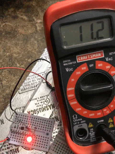
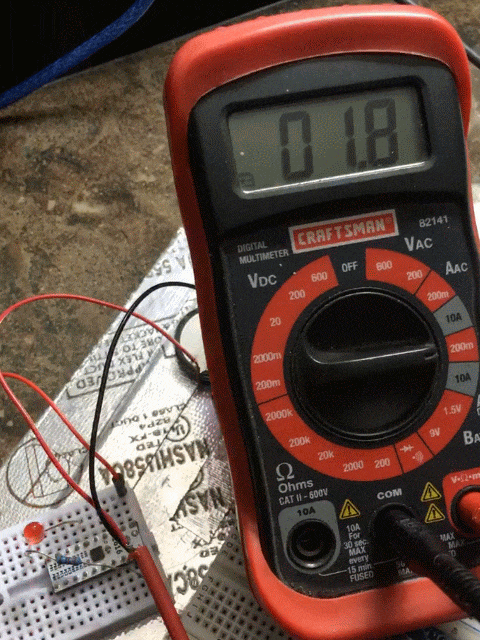
#include <avr/sleep.h>

void RTC_init(int RTCdelay)
{
  RTC.CLKSEL = RTC_CLKSEL_INT32K_gc;    // 32.768kHz Internal Crystal Oscillator (INT32K)

  while (RTC.STATUS > 0);               // Wait for all register to be synchronized
  RTC.PER = RTCdelay;                   // Set period for delay
  RTC.INTCTRL |= RTC_OVF_bm;            // Enable overflow Interrupt which will trigger ISR
  RTC.CTRLA = RTC_PRESCALER_DIV32_gc    // 32768 / 32 = 1024 (sec) ~ 1 ms
  | RTC_RTCEN_bm                        // Enable: enabled
  | RTC_RUNSTDBY_bm;                    // Run In Standby: enabled
}

ISR(RTC_CNT_vect)
{
  RTC.INTFLAGS = RTC_OVF_bm;            // Clear flag by writing '1'
  digitalWrite(LED_BUILTIN, CHANGE);
}

void setup()
{
  pinMode(LED_BUILTIN, OUTPUT);
  RTC_init(1000);   // Start the RTC time counter, counting up to 1000 (~1 sec.)

  set_sleep_mode(SLEEP_MODE_STANDBY);  // Set sleep mode to STANDBY mode
  sleep_enable();
}

void loop()
{
  // nothing to do here
  sleep_cpu();
}
You can use a voltmeter to measure the current before and after these changes.
![]()
You will notice that the current when the LED is off will go from 11.2mA to about 0.5mA.
![]()
A great improvement, but we should be able to go below 20μA. Writing a similar code on Atmel Studio did indeed drop it down below at least 0.1mA (my cheapo voltmeter is not measuring low enough).
![]()
It looks like the current Arduino Core has some peripherals running which we should turn off before entering the sleep mode. That is currently beyond the scope of this log, but I will update later when I find a solution.
-
Setting up channels for the Analog-to-digital converter (ADC)
07/04/2019 at 04:28 • 0 commentsIn one of the earlier logs PORT was explained, but that can only be used for digital I/O, meaning, it can turn outputs on or off, or detect if an input is on or off. The actual pin number for digital I/O consists of a PORT letter followed by a pin (or bit #) in that PORT. Every non-power related leg (like VDD and GND) on the ATtiny is linked to one of those PORTS, but that is usually not the only function of that leg.
The Analog to Digital Converter (ADC) is a great feature on the MCU to measure input voltage. Instead of using PORT to link a the digital I/O to the leg, it uses channels. The ATtiny1616 has 12 input channels (AIN0 to AIN11) on two ADC’s (ADC0 and ADC1). The location of these input channels (we are going to use ADC0 only) are as follows:
//                          _____
//                  VDD   1|*    |20  GND
// (nSS)  (AIN4) PA4  0~  2|     |19  16~ PA3 (AIN3)(SCK)(EXTCLK)
//        (AIN5) PA5  1~  3|     |18  15  PA2 (AIN2)(MISO)
// (DAC)  (AIN6) PA6  2   4|     |17  14  PA1 (AIN1)(MOSI)
//        (AIN7) PA7  3   5|     |16  17  PA0 (AIN0/nRESET/UPDI)
//        (AIN8) PB5  4   6|     |15  13  PC3
//        (AIN9) PB4  5   7|     |14  12  PC2
// (RXD) (TOSC1) PB3  6   8|     |13  11~ PC1 (PWM only on 1-series)
// (TXD) (TOSC2) PB2  7~  9|     |12  10~ PC0 (PWM only on 1-series)
// (SDA) (AIN10) PB1  8~ 10|_____|11   9~ PB0 (AIN11)(SCL)
So as you can see a leg could have be a digital pin (for example PA4) and an analog input (AIN4). Like the digital I/O we are going to tell Arduino which pin# is linked to each analog channel as follows in pins_arduino.h:
#define digitalPinToAnalogInput(p) ((p<6)?(p+4):(p==17?0:((p>13)?(p-13):((p==8)?10:(p==9?11:NOT_A_PIN)))))Big thanks to Spence Konde! He helped enormous in creating all the pre-processor macros. But newbies, like me, are probably wondering what this line above is doing.
We are all familiar with an if statement, for example:
if(p < 6) {
    p = p + 4;
} else {
    P = NOT_A_PIN;
}
There is actually a shorter method writing the same if statement above, for example as follows:
p = (p<6)?(p+4):NOT_A_PIN;
Using this same method for the macro above will result in the following if statement:
if(p < 6) {
    digitalPinToAnalogInput(p) = p + 4;
} elseif (p == 17 {
    digitalPinToAnalogInput(p) = 0;
} elseif (p > 13 {
    digitalPinToAnalogInput(p) = p-13;
} elseif (p == 8 {
    digitalPinToAnalogInput(p) = 10;
} elseif (p == 9 {
    digitalPinToAnalogInput(p) = 11;
else {
    NOT_A_PIN
}
With “p” being the Arduino pin number, we can now determine which channel belongs to that pin with the macro above. For example when p=5 (leg #7), digitalPinToAnalogInput(p) will be 5 + 4, resulting in channel 9.
You can just read the voltage on the input pin by entering the following in Arduino:
analogRead(5) // reading the analog input on channel 9.But most Arduino’s have a dedicated section for analog inputs, for example on the Arduino UNO A0 up to A5 are used as analog inputs. In order to use these A0, A1 etc numbers we have to add these with macros to the pins_arduino.h as well as follows:
#define PIN_A0   (17)
#define PIN_A1   (14)
#define PIN_A2   (15)
#define PIN_A3   (16)
#define PIN_A4    (0)
#define PIN_A5    (1)
#define PIN_A6    (2)
#define PIN_A7    (3)
#define PIN_A8    (4)
#define PIN_A9    (5)
#define PIN_A10  (10)
#define PIN_A11  (11)

static const uint8_t  A0 = PIN_A0;
static const uint8_t  A1 = PIN_A1;
static const uint8_t  A2 = PIN_A2;
static const uint8_t  A3 = PIN_A3;
static const uint8_t  A4 = PIN_A4;
static const uint8_t  A5 = PIN_A5;
static const uint8_t  A6 = PIN_A6;
static const uint8_t  A7 = PIN_A7;
static const uint8_t  A8 = PIN_A8;
static const uint8_t  A9 = PIN_A9;
static const uint8_t A10 = PIN_A10;
static const uint8_t A11 = PIN_A11;
Instead of only using the pin#, now analogRead(A9) can be used as well, resulting with the same readings.
In the next log I will explain the internal voltages which can be used to get a reliable analog input reading.
-
Using voltage reference for ADC
07/04/2019 at 23:14 • 0 commentsWe probably all got to a point where we must start using a multi-meter to analyze our circuit, and very often we want to measure the voltage. Putting one of the probes on voltage source will not give us any feedback, the second must be connected to a reference and in most cases that will be the ground.
Analog-to-digital converters (ADC) work very similar. They can take a voltage, for example from one of the pins, and calculate a difference to another reference. There is just one little difference here. The voltage we like to measure must be lower than the voltage on the reference. For example, when we like to measure 5V, we need at least 5V as a reference. Reason is that we are measuring a fraction as follows: Vin / Vref. So when Vin is 5V, and Vref is 5V, we will get 1 back. On the other hand when Vin is 1V, and Vref is still 5, we will get 0.2 as a result.
So the ADC calculates a fraction, but the microcontroller cannot hold fractions, it calculates in bits. The ATtiny is using a 10 bit register to hold this value between 0 and 1 using these 10 bits. In decimals 10bits can hold a value of 2^10 – 1024, but since we start at 0 the maximum decimal value is 1023. Using that conversion, to go from a fraction to bits, will result in the following equation:
You can find some information on this equation in the data sheet on page#485:
http://ww1.microchip.com/downloads/en/DeviceDoc/ATtiny3216_ATtiny1616-data-sheet-40001997B.pdf
If the Vin is above Vref, for example Vin is 5.5V and Vref is still 5, the ADC will result with the maximum 10bits value of 1023. According to the equation this should result in 1125, but since we can only have 10 bits we will only get a value up to 1023 instead.
Most used Vin is the analog input pin, on the Arduino UNO pins A0 to A5, and the Vref will be the applied voltage (3.3V or 5V). But there are tons of more combinations possible! Lets start with Vin on page# 495 of the datasheet. This is very similar to the PORTMUX where from an earlier log where we told the controller which serial ports we like to use. In this case we must tell the ADC what we like to convert. Starting at the top you can find AIN0 which the Analog Input Channel linked to a pin (explained in the previous log). Besides the pins we also have other options starting at 0x1B. PTC, DAC0, INTREF and GND. Later I will show an example where we can use these.
Secondly, we need the V reference and there we have tons of options as well. You will find those on page#491 Bits 5:4 REFSEL. It will get a little bit confusing here! There is not just one Vref. There is one for the ADC, DAC and the AC. so from now on I will call it ADC0.Vref. As you can see there are only 3 options for the reference. INTERNAL, VDD and VREFA. VDD is the applied voltage, so when you apply 5V to the microcontroller, VDD is 5V. Another option is applying an external voltage on VREFA, which is located on pin#1 in this situation. VREFA has nothing to do with VREF, it is just another reference for the ADC. The INTERNAL option is even more interesting. It uses the internal reference voltage of the chip, Vref, but again has nothing to do with ADC0.Vref, unless this INTERNAL option is selected. The Voltage Reference VREF is explained in chapter 18 where you see that it has 5 different settings:
- 0.55V
- 1.1V
- 1.5V
- 2.5V
- 4.3V
Using the INTERNAL voltage reference can be helpful when you VDD is not consistent but you want a consistent reading from an external voltage source.
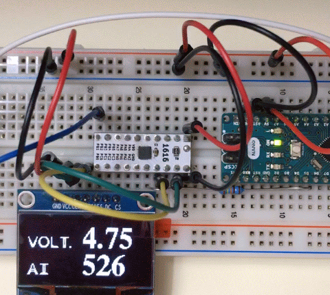
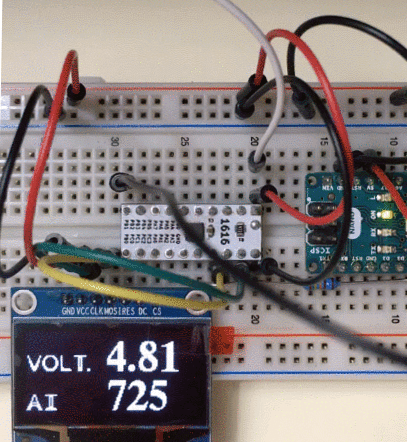
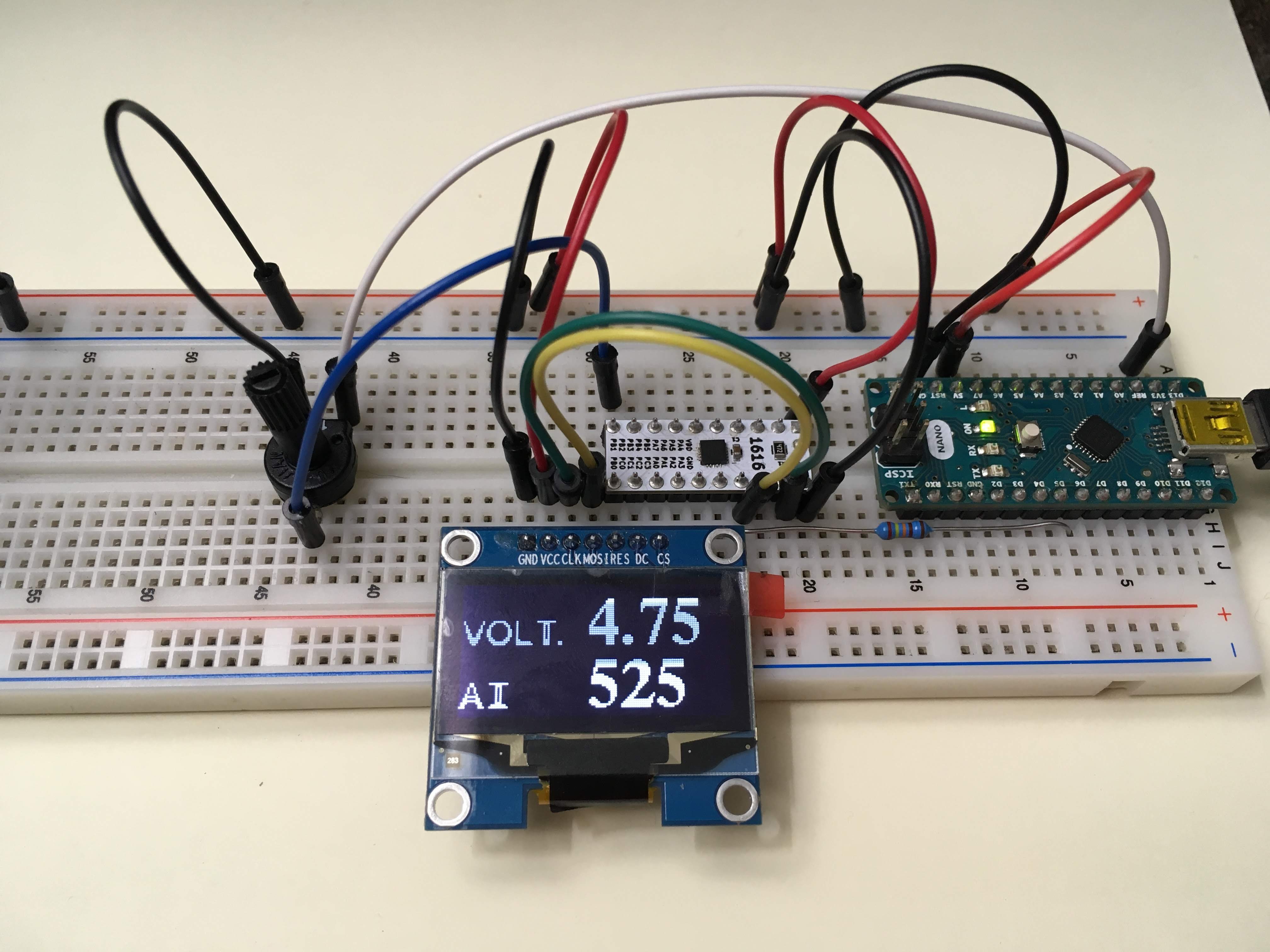
In the following examples I will use a super capacitor as a power source to the ATtiny1616. The voltage from the super capacitor will drop as soon as it disconnects from the 5V source used to charge the super capacitor. Measuring the incoming voltage on the ADC from different sources requires different solutions as follows:
![]()
Reading a potmeter attached to VDD. This is very common when using the Arduino. When we turn the pot right in the center, we will get 2.5V when we use a 5V source, but only 1.65V when we use 3.3V. This will result in the following:
And for the 3.3V version:
![]()
That is great! The actual analog reading is not changing when the voltage is changing, but there are other situations, for example: We have a voltage coming in from another device telling us the temperature by sending a voltage between 1-4V. Before we used Vref (the VDD) as a reference for the analog input, but our VDD voltage is dropping from 5V to 3V, this will result in reading higher values coming in till the VDD drops below the incoming voltage and it only reads 1023 max. For example, we have a constant 2.5V provided by a sensor, resulting in the following reading when the super capacitor is fully charged:
But now our voltage is dropping, till 1.8V and the microcontroller will turn off, results into the following reading:
Since 1420 is above 1023, the actual reading of the analog input will be 1023. The actual readings are changing constantly as shown in the video below:
![]()
So in order to get a stable reading we must change the ADC0.Vref to INTERNAL and pick one of the voltage references, in this example 1.1V. In Arduino the following command will do both:
analogReference(INTERNAL1V1);
analogReference(INTERNAL1V1);
other options are:
INTERNAL0V55
INTERNAL1V1
INTERNAL2V5
INTERNAL1V5
INTERNAL4V3
VDD
EXTERNAL
We are going to use 1.1V as the reference since we know that the voltage supplied by the super capacitor will drop as low as 1.8V, which is the minimum voltage requirement for a stable Vref of 1.1V. All the higher voltages will be useless when the VDD gets that low. But the analog input is still reading 2.5V, resulting in:
So in order to use the internal reference we have to use a voltage divider to make sure the voltage on the analog input is below the internal voltage.
![]()
I use a potentiometer on the incoming voltage to bring it down to a usable reference voltage, in this case down to 0.56V:
Since we no longer have a reference to VDD, the analog input is consistent even when the voltage is dropping:
![]()
ATtiny 1-series with Arduino support
Creating a break-out board for the ATtiny1616 where sketches can be uploaded from Arduino with the Arduino UNO or a modified AVR JTAG ICE