 Jacob Still
At the end of the last post, I said that this one would be on programming. Sorry to disappoint, but this is not about programming. This is about putting the prototype circuit boards together
I received the circuit boards and just about ripped them open as the postman was giving them to me. In the mail came two boxes, one with the vacuum sealed PCBs and the other with the massive solder stencil. When I ordered, I didn't realize that the stencil was going to be so big, oh well.
Massive stencil:
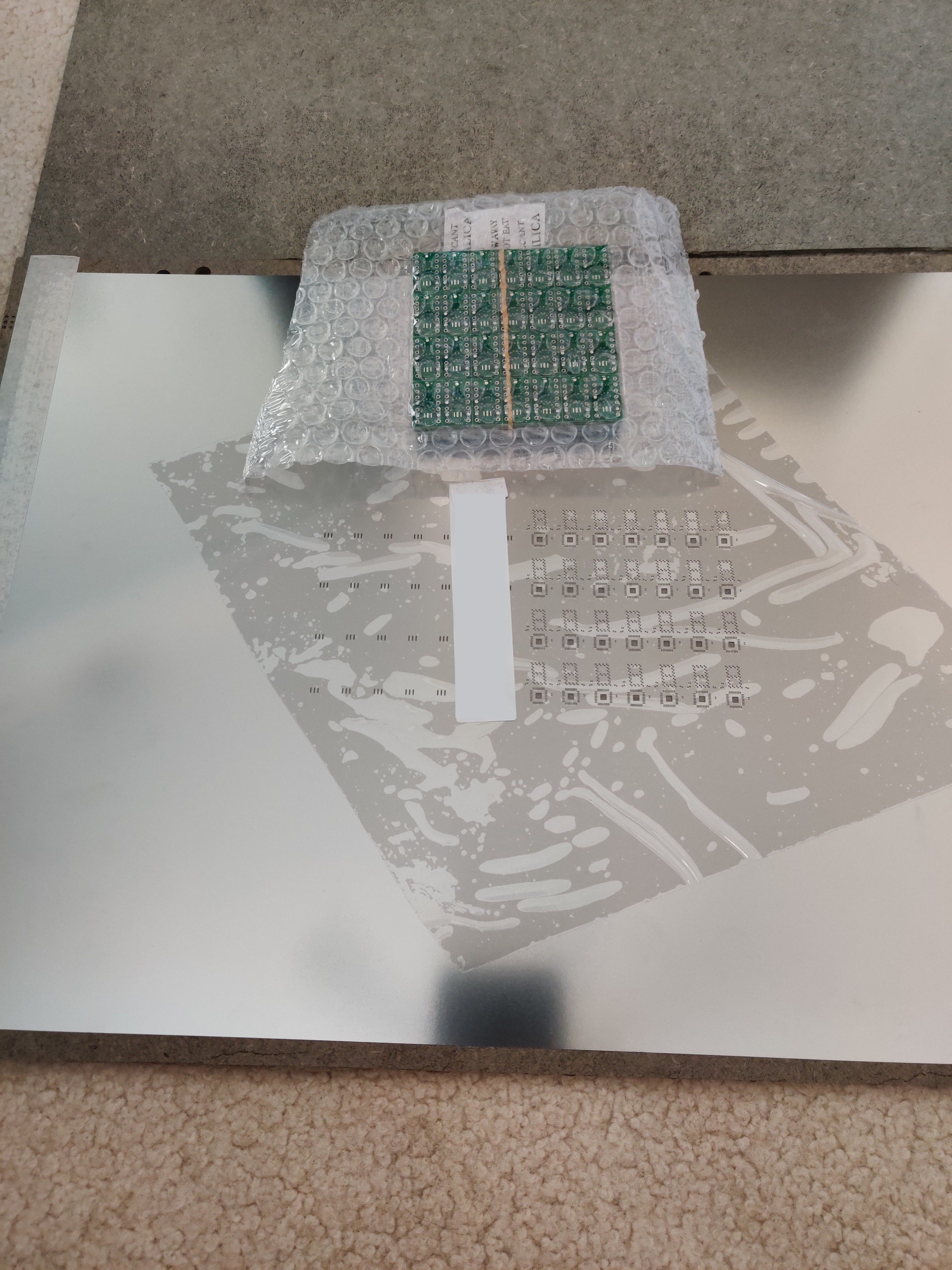
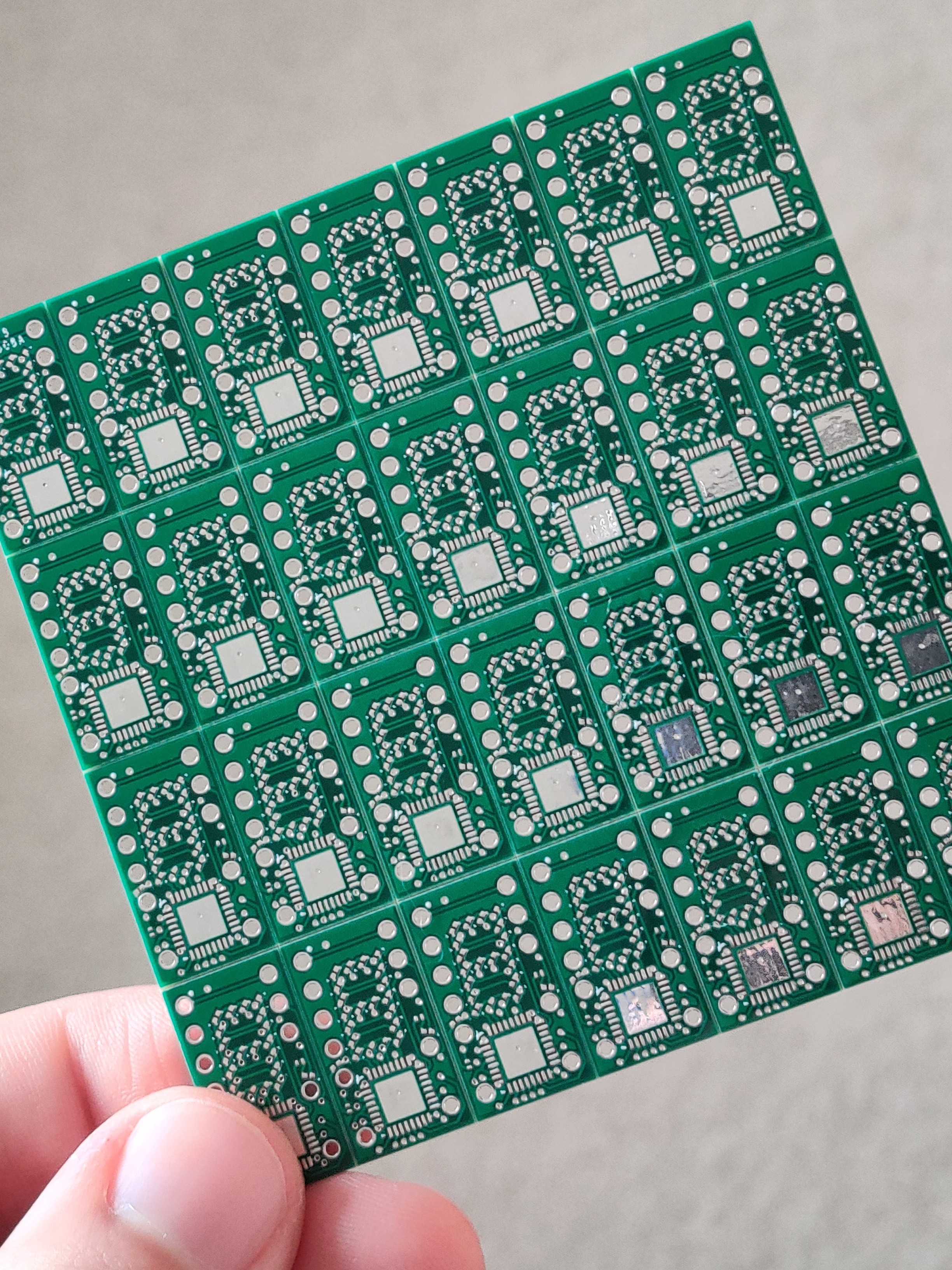
These boards are Tiny:
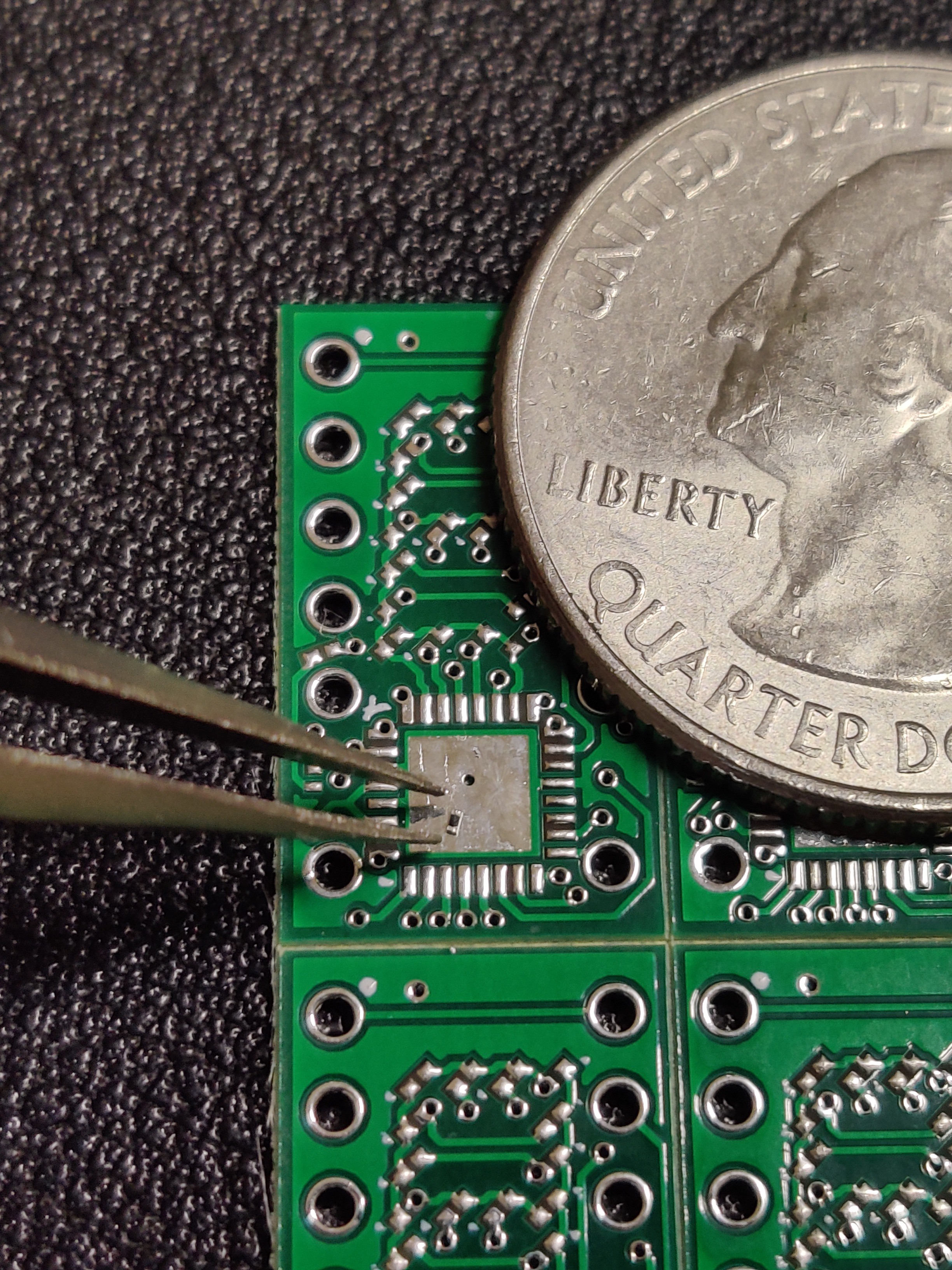
As soon as I opened the boxes, the realization of just how small these things are set in. The microscopic size is daunting. Yes daunting. There are a total of 81 pads per board including the relatively massive ground pad under the processor, all of which are less than a millimeter in size, except the ground pad.
I have opted to go from easy mode - soldering large through hole components, to Super Uber Brutal Extreme Mode (SUBEM™) - soldering the absolute smallest components I could find BY HAND. This is mainly because I hate myself and like to suffer (i.e., space on the board was at a premium).
28 pc. panel of the tiny DIYTIL311s:
Solder Testing:
Soldering is pretty straightforward. I didn't get a picture, but after taping down a couple boards to use as a guide, I put the board to be soldered down and lined up the stencil. Using an old gift card, I scraped the solder paste across the stencil and removed it. The result was fairly good.
Wet solder paste:
This was my first time using solder paste, stencil and a hot air station. Because of this, I decided to use the first board as a test to see how good the stencil really worked. You can see in the picture above that the pads for the LEDs look to have good coverage, but the processor's pads are kind of overlapping. This is ok as the surface tension of the liquid solder will cause it to flow onto the pad. In the picture below, you can see that some of the pads of the processor have "bridged" across. This will not be an issue once the part is sitting on the pads as the solder will have to cover more surface area and will be sort of pulled away from these points due to surface tension.
After flowing the solder (first row of boards only):
Soldering the Prototypes:
I spent maybe an hour placing all the components. Because of the size, they tend to stick to the tweezers when trying to push them around or place them. It took some time to be able to place something this small. Thankfully, the flux inside the solder paste helped to hold the components while placing them.
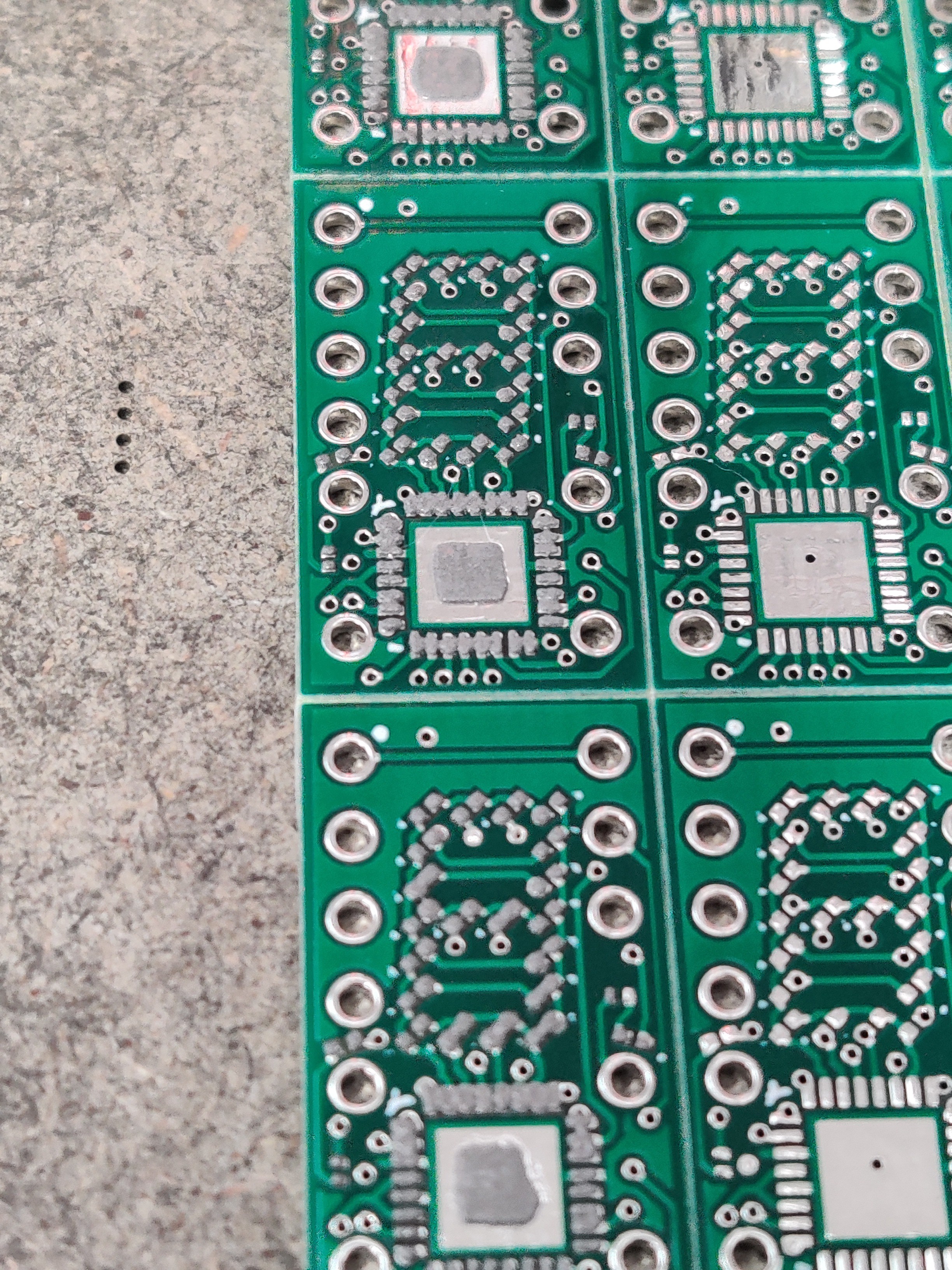
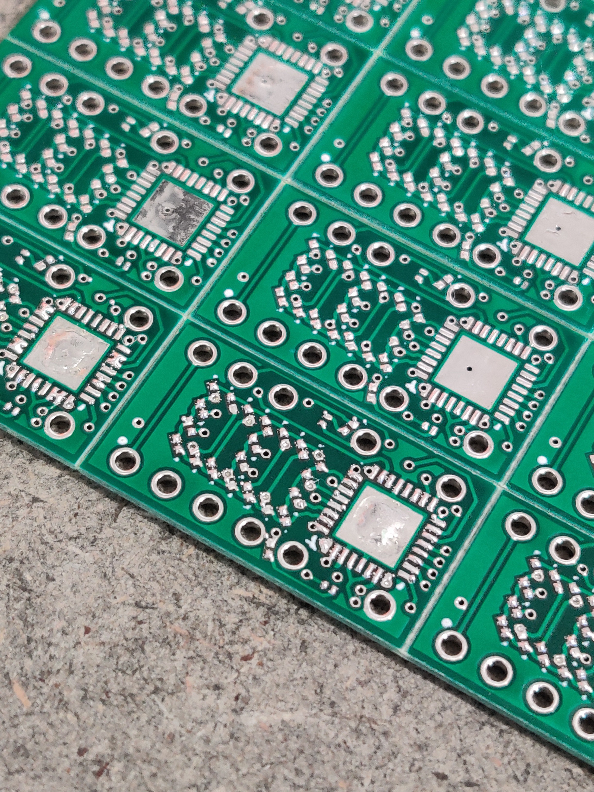
I would just like to point out just how small these components are:
LEDs Placed:
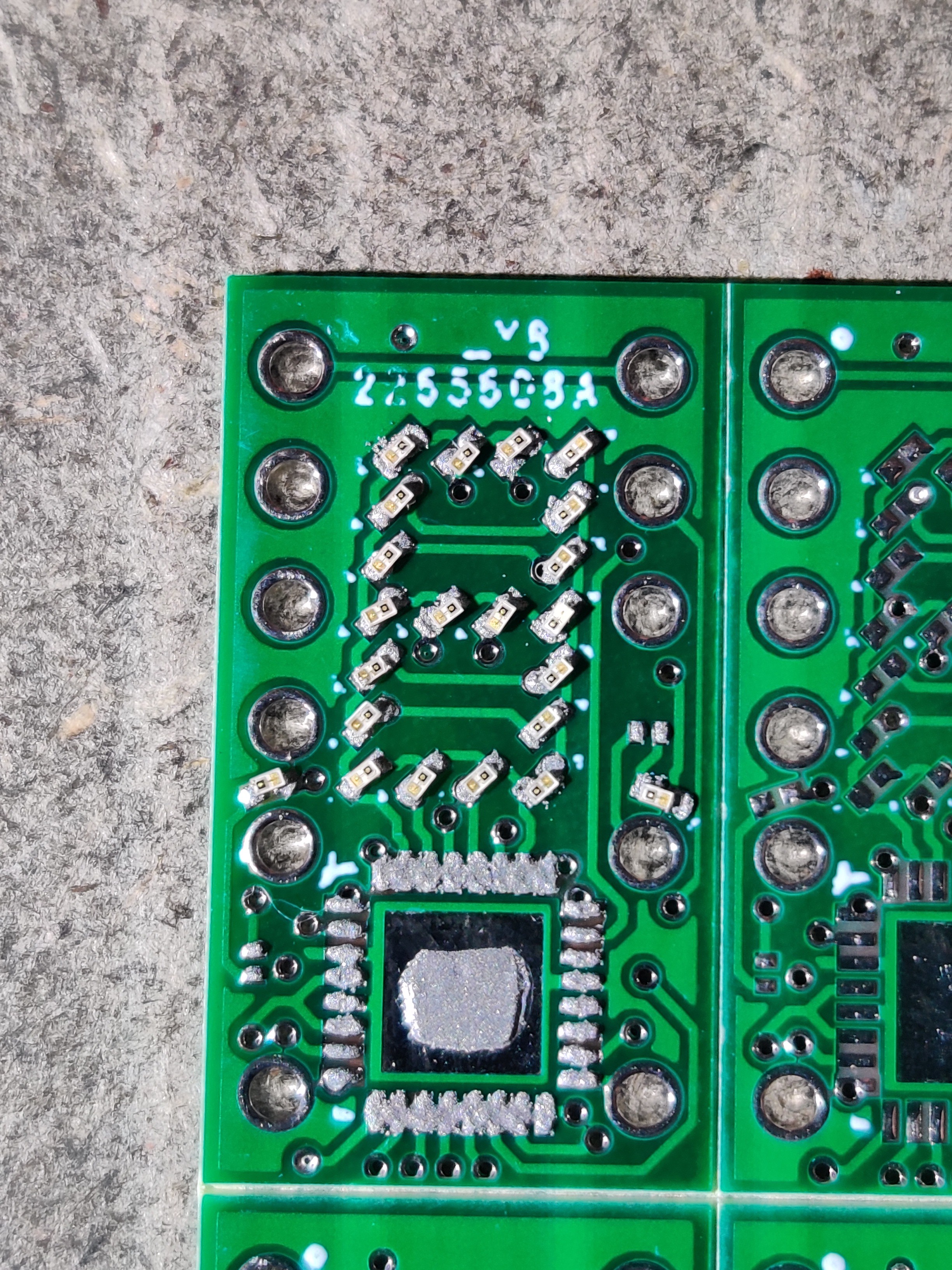
Resistors and Processor placed on board:
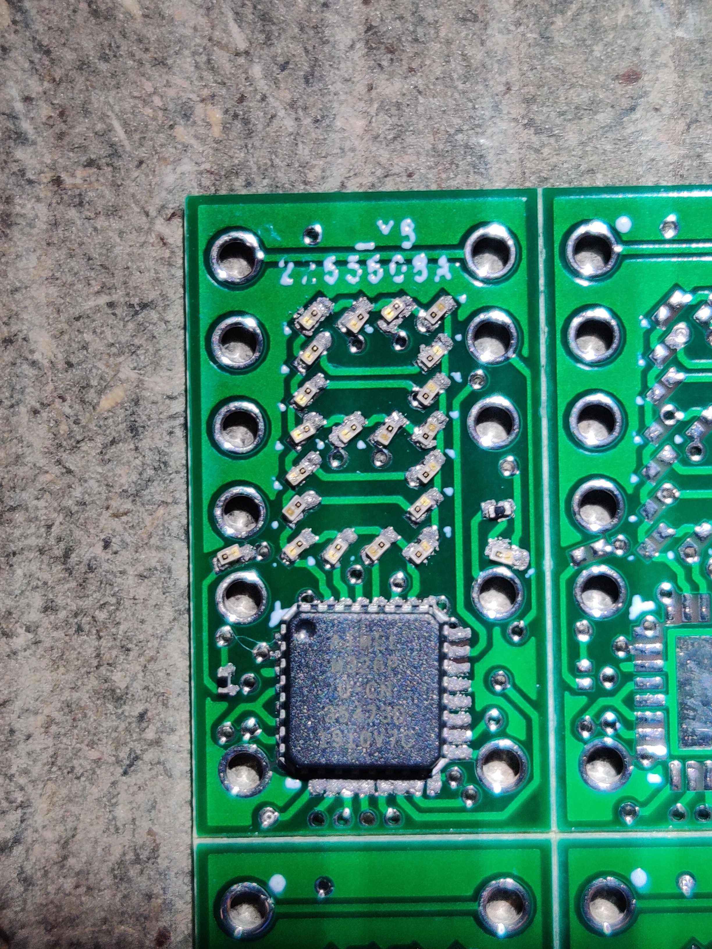
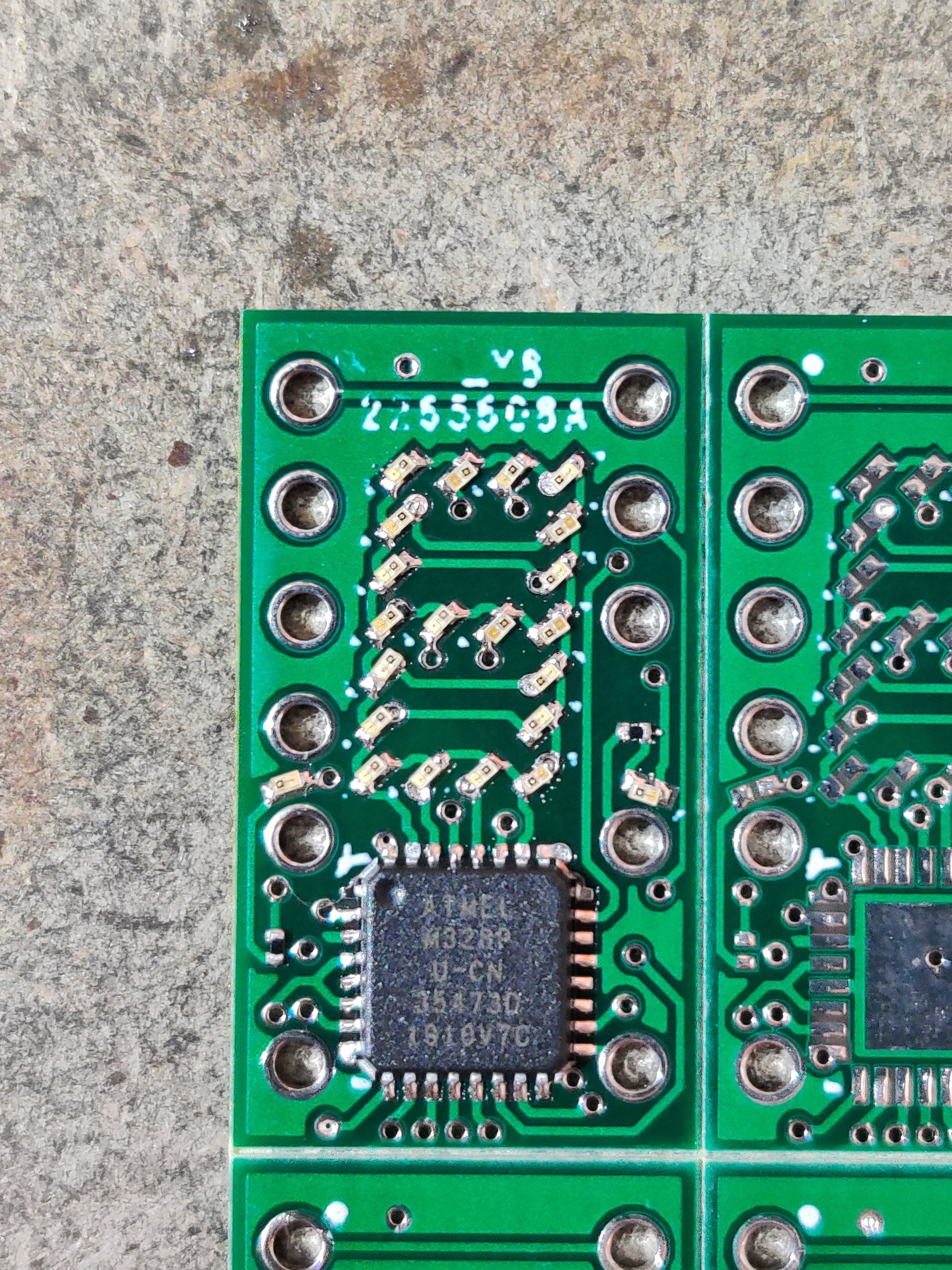
Final board after flowing the solder and convincing some of the parts around:
Soldering the pins:
I want this to be as accurate to the original as possible, so I made a jig to help solder pins. This way the black plastic part found on male headers won't be on the board. The jig was built from both male and female headers laying around. Pins are then put into the holes and pushed all the way down. This is to have the pins sticking out on top of the board be as short as possible. The jig is to make soldering easier but also to hold the pins perfectly straight during soldering. I used one of the boards that I tested the solder on for testing the pins as I only have enough components to make three prototypes for now and I don't want to mess up and have to scrap one.
Pin Soldering Jig:
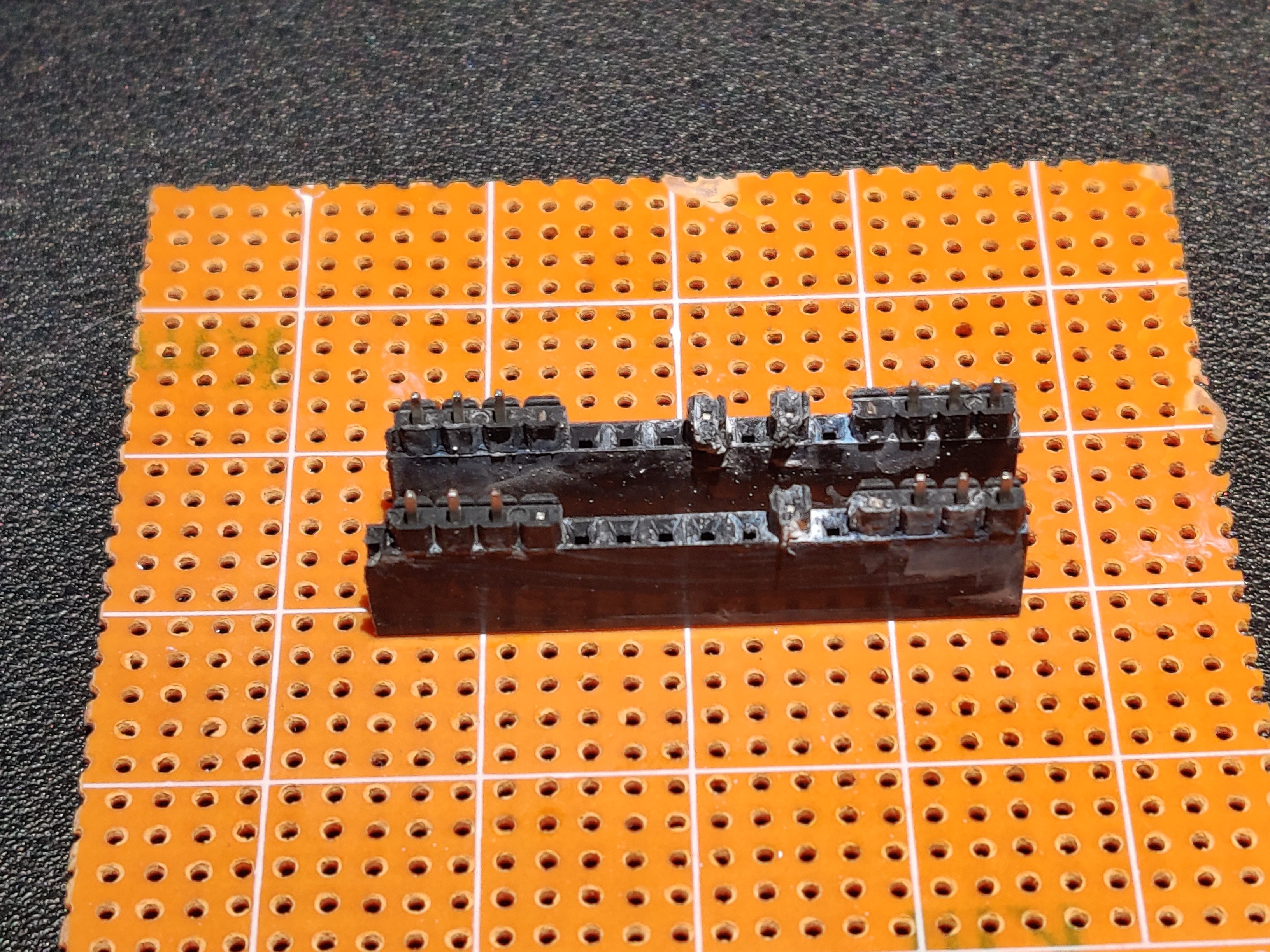
The pins put on holes:
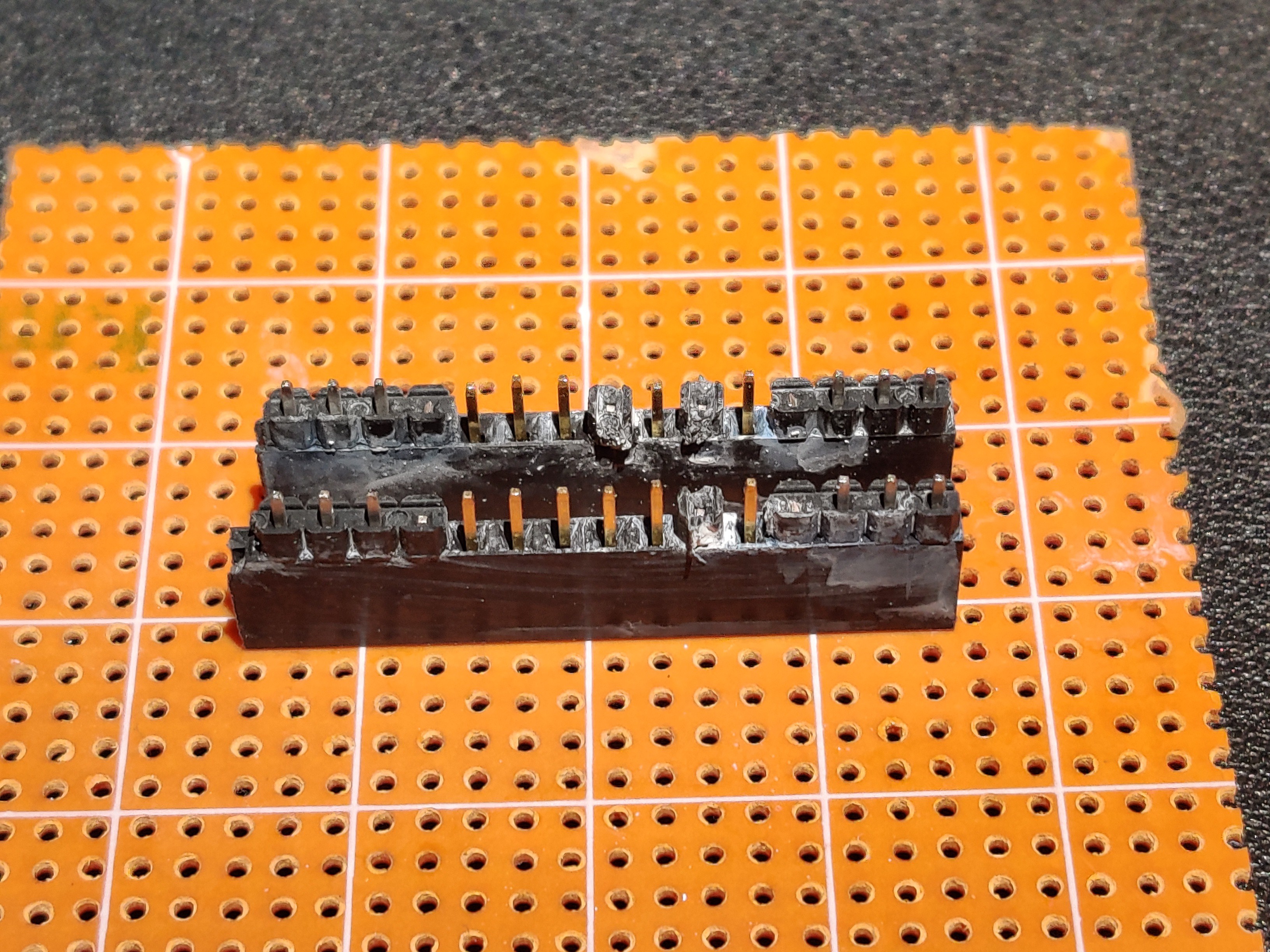
Board Placed and Soldered:
The result is perfectly straight pins:
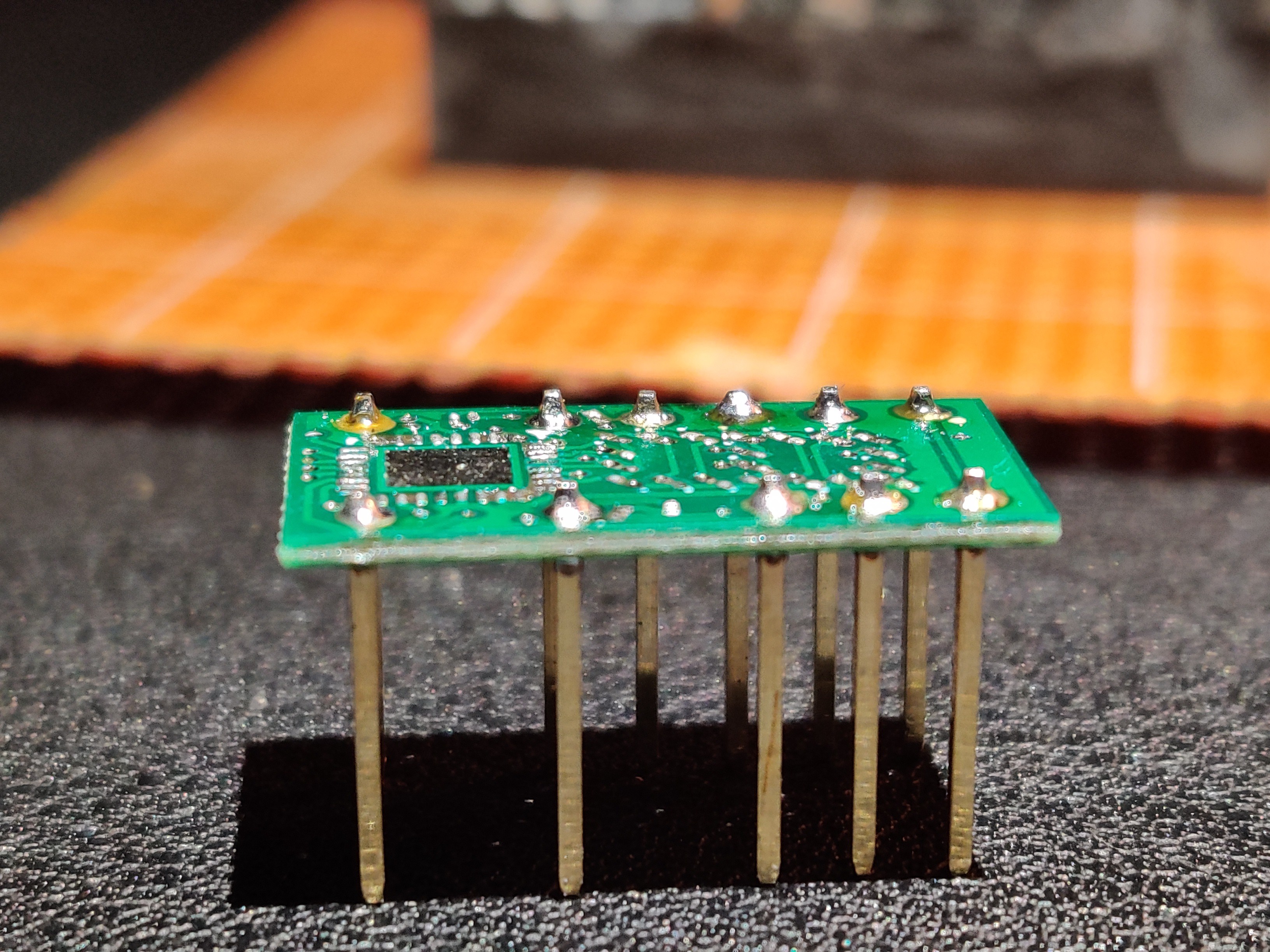
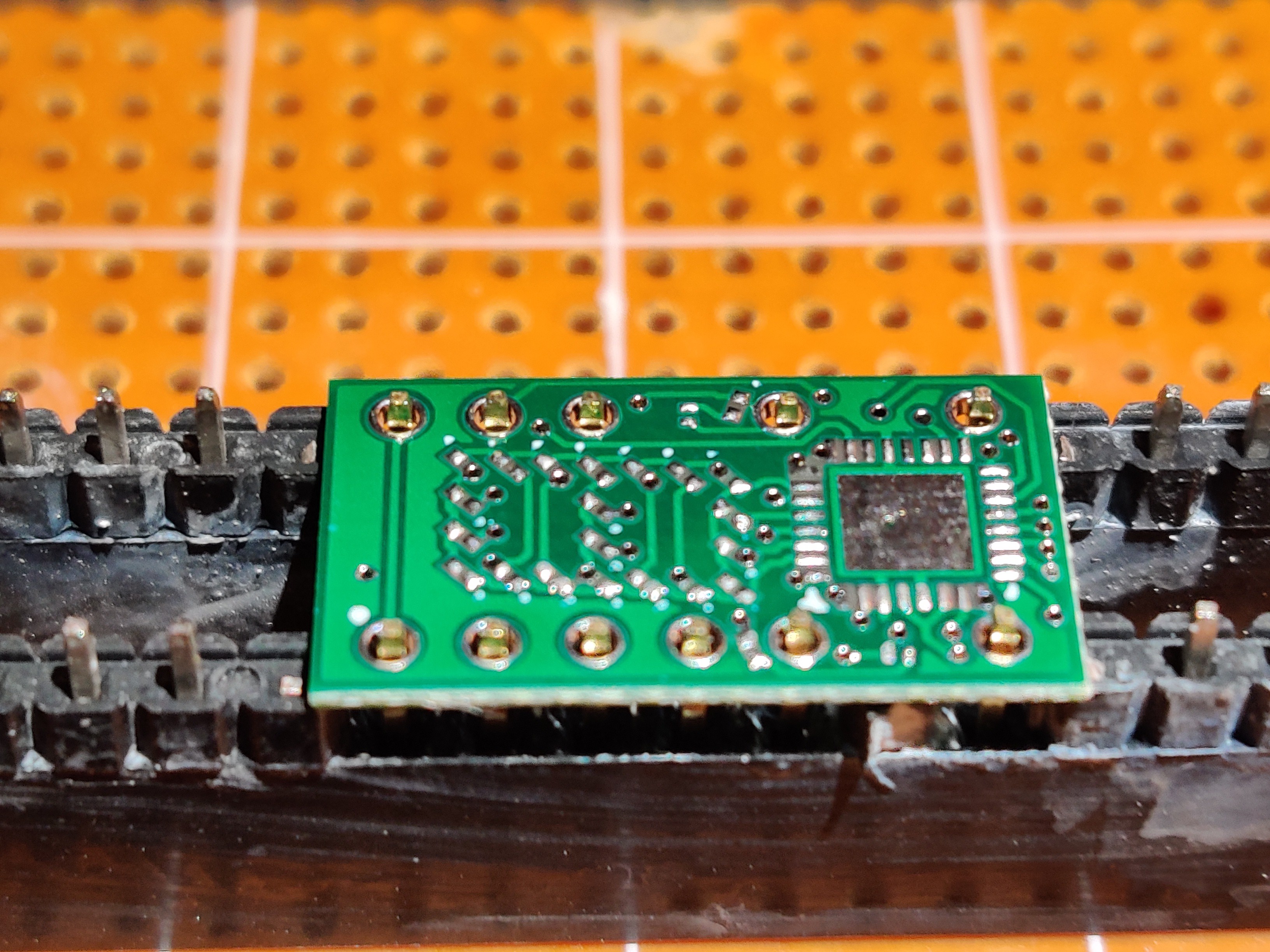
There is a height problem though:
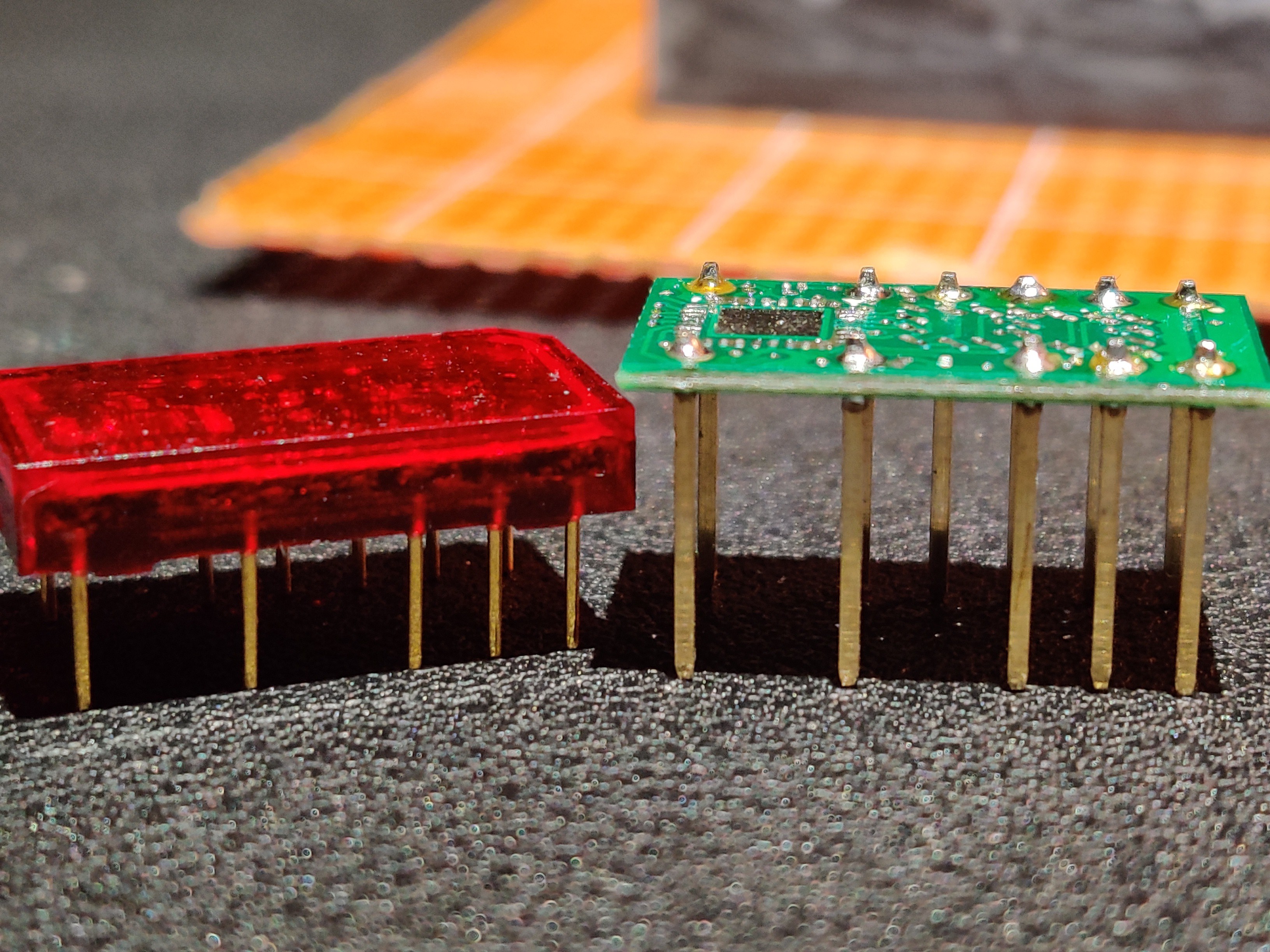
I am exploring options for shorter pins. I think the most viable option is to do what Alex did at the center of this page. I am open to other suggestions for making the pins shorter for relatively cheap and little effort (I won't cut every pin in half if I don't have too).
Discussions
Become a Hackaday.io Member
Create an account to leave a comment. Already have an account? Log In.