 Shyri Villar
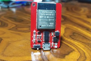
The device is basically an ESP32 connected to the GBA through the link port. With the device connected and without any cartridge inserted in the GBA, once the GBA turns on the ESP32 sends a small rom to be loaded in the GBA. This rom is a program made to enable communication between the ESP32 and GBA for both handling bluetooth connection and sending the user input to the ESP32 when it is connected to a bluetooth host and act as a gamepad. Unfortunately it only works with traditional GBA and I couldn't make it work with GBA SP. I think GBA SP just doesn't give enough power.
When turned on the ESP32 performs a multiboot sequence through the SPI to the GBA sending a rom that the ESP32 has stored in the flash memory. Once loaded the ESP32 enables the UART port in the same pins and the rom communicates with the ESP32 using UART through the link port.
The ESP32 is powered by the 3.3V the GBA gives through the port
---------------------------------------------------------------------------------------------------------
Previous version of this project used an Atmega and an HC-05. This is the description for that prototype:
A GBA program that uses the link port to communicate with a HC-05 bluetooth module using UART (HC-05 flashed with RN-42 firmware, find how to do it in the links at the bottom).
This rom is stored in a W25Q32 flash chip. An Atmega328P performs a multiboot sequence reading from this chip and sending to the GBA through the link port.
Once multiboot ends, the gba program runs and talks to the HC-05 to handle bluetooth connection, and key presses.
Additional 74XX157 quad 2-input multiplexer makes possible to multiplex SPI to read from the flash chip and send the multiboot, it alternates byte reads from the flash chip and send them to the GBA. Then using hcf4066 switch link port pins are switched from the spi to the HC-05 uart pins.
The whole circuit runs at 3.3V provided by GBA through the link port.
Final version of the circuit includes a 6 pin port that allows to reprogram the atmega if necessary. Also it lets to turn the atmega into a special write mode to reprogram the flash memory.


 SAYANTAN PAL
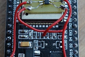
 anlumo
Hi Shyri. If you read this, I’ve been able to get the ESP32 version working up to the point where I connect it.
On OS X I can’t figure out if it’s making any inputs, any ideas? On my primary Windows machine I need to upgrade to Bluetooth 4.2+ before I can try debugging on there. I currently only get a driver error when I try to connect, best guess is at the error is the ESP32 is bt4.2 and my PC dongle is 4.0.
Love this project. Cheers!