 Adrian.l.west
Introduction:
You probably clicked on this thinking holy cow, 500 AMPS!!!!!. To be honest, the MOSFET board I designed will not be able to safely do 500Amps. It might for a short bit, just before it excitedly burst into flames.
This was not designed to be a clever trick. It was NOT my evil plan to lure you into my page (insert mad scientist laugh here). I wanted to make a point. The advertising for 3D printers and their components can be very misleading. Especially in the low cost DIY market.
I'm going to explore just one case of this. A common MOSFET board which is used to protect the 3d printer main board from damage. They are also used to upgrade a pinter to a more powerful headed bed. Generally with more print area.
There are half dozen different designs out on the market. Most have these giant heatsinks and look very impressive. But most of that is a gimmick.
While we analyze one of these boards; I am going to design my own. After looking at what's on the market, I decided I could do better. So, I am Open source, Open Capabilities, and does the job exceedingly well.
The design I am targeting is a 40v 60Amp dual MOSFET board. Not 1 channel but 2. One for the heated bed and one for the hotend. There is a story behind the design. For those of you who don't care about the story behind the board, you can go straight to the source files for the board.
Tools:
- Tweezers
- Soldering iron
- Solder
- Snips for Electronics
BOM:
| References | Supplier Part No | Supplier | Value | Quantity |
|---|---|---|---|---|
| C11, C21 | CL21B103KBANNND-ND | Digi-Key | 10000pF | 2 |
| R11, R21 | 311-1.00KFRCT-ND | Digi-Key | 1.0K | 2 |
| R15, R25 | 311-3.60KFRCT-ND | Digi-Key | 3.6K | 2 |
| R13, R23 | RMCF1210JT2K00TR-ND | Digi-Key | 1.99K | 2 |
| D11, D21 | BZX84C15LT3GOSTR-ND | Digi-Key | 15V | 2 |
| U11, U21 | TLP182(BL-TPLECT-ND | Digi-Key | TLP182 | 2 |
| CN11, CN21 | 277-1667-ND | Digi-Key | 2 | |
| Q11, Q21 | AUIRFSA8409-7P-ND | Digi-Key | AUIRFSA8409-7P | 2 |
| J11, J21 | PRT-10474 | Spark Fun | XT-60-M | 2 |
| J12, J22 | PRT-10474 | Spark Fun | XT-60-F | 2 |
| JUMPERS | 10 AWG solid core wire | Local HW Store |
Given the Facts But It Does Not Represent What You Are Purchasing:

The MOSFET board in that picture is very common. You can find it on eBay, Ali Express, Amazon and loads of other places. It's also very inexpensive. For 2 you could pay as little as $5.00.
The Headline usually is "210 Amp MOSFET". It is true that the MOSFET is a 210 amp MOSFET. However, the entire product can only do 25 Amps. The limiting factor is the PCB and the connector.
As we'll see later, The PCB probably limits the design even more. The copper traces don't look very thick.
So they told you the truth about the MOSFET but not about the entire product.
There's also a lot of marketing going on here. See that giant heatsink. Most people think wow that must be a pretty powerful part. The truth is, if that part NEEDS that heatsink the MOSFET is wasting a lot of energy. That energy could have gone into heating the print bed. A large heat sink is not a good sign. But it is what we expect to see on high power devices. The best I can tell this part is just for marketing, at least at 25 Amps.
I want to design a product that does it's job well, is good quality, low cost, and is very straight forward about its capabilities.
The Core of the Circuit: the MOSFET

I want the design to be very efficient. That would mean low power loss across the device. So resistance is my enemy. MOSFETs act like a voltage controlled resistor. So when they're off, their resistance is very large. When they're on, their resistance is very low. There's actually a lot more going on than that. However, for our discussion it'll be good enough.
The parameter we should pay attention to on MOSFET data sheet is "RDS on".
The MOSFET I selected was the AUIRFSA8409-7P made by Infineon Technologies. It's worst case RDSon is 690u Ohms. Yep, that was correct micro...
Read more »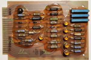
 Skyhawkson
 Ray Olsen
 Jeremy Gilbert