Part - I Real-Time oscilloscope
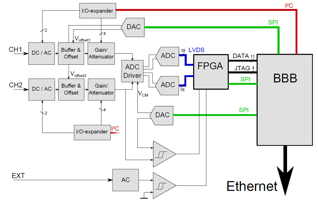
A. Analog front-end and ADC
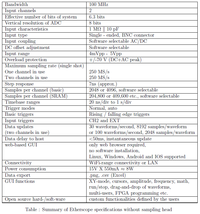
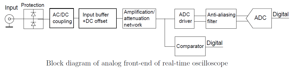
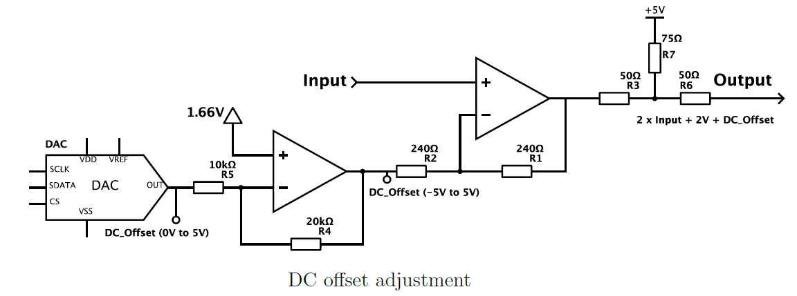
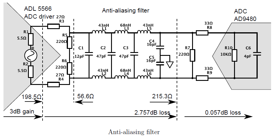
The input circuit features an input impedance of 1 M || 10pF and overvoltage protection. The DC/AC selection, DC offset adjustment, gain/attenuation (vertical division), trigger source selection etc. are supported by the ebbased GUI (graphical user interface). An 8-bit, monolithic analog-to-digital converter (ADC) converts the analog signals to LVDS (Low-voltage differential signaling) digital outputs at a sampling rate of 250 MS/s. A seventh-order Butterworth anti-aliasing filter is implemented between ADC driver and ADC, aiming to eliminate unwanted, spurious out-of-band signals.
B. FPGA
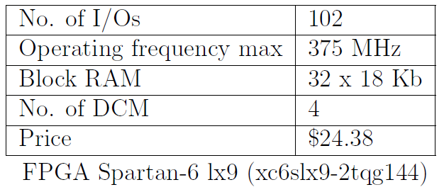
Spartan -6 FPGA delivers an optimal balance of low risk, low cost, and low power for cost-sensitive applications. The FPGA can have abundant Block RAMs as data buffer or FIFO (First in, first out) to store the data acquired by the ADCs and abundant IOs (LVDS IOs) making it possible to handle the ADC LVDS outputs in parallel, and to make a fast, parallel communication link with the PRU (Programmable Real-Time Unit). The paramount aspect of an FPGA is the parallelism, which implies that the communication with Beaglebone Black, the interfacing of ADCs and the data transfer to PRU can be performed simultaneously. This unique aspect ensures the high performance and robustness of the system.
C. Beaglebone Black and PRU
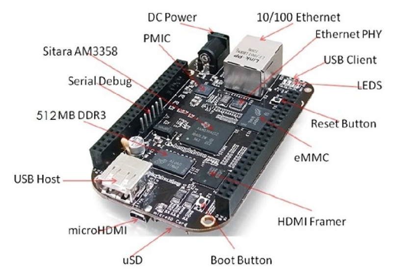
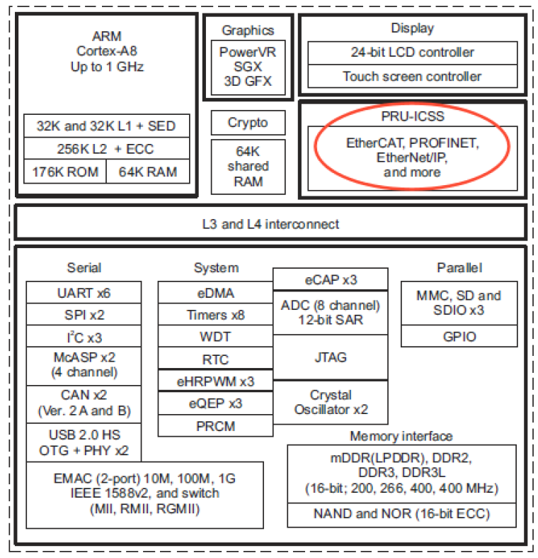
The BeagleBone Black, newest member of the BeagleBoard family, is a credit-card sized, low-power, openhardware computer. It is community-supported development platform for developers and hobbyist and it runs on Linux and boots under 10 seconds. Unlike other similar devices, it does offer good access to most PRU or microcontroller pins, as required for hardware extension. The Programmable Real-Time Unit and Industrial Communication Subsystem (PRU-ICSS, embedded in Beaglebone Black processor) consists of dual 32-bit RISC cores (Programmable Real-Time Units, or PRUs), shared memories, and instruction memories etc. The PRUs can operate independently or in coordination with each other and can also work in coordination with the device-level host CPU, making it possible to set up a custom and independent communication link with FPGA.
D. Web-based software
The GUI is embedded in a dynamic web page (programmed in HTML and JavaScript) with the help of
Node.js library. This Node.js application is designed not only to maximize the throughput and efficiency but also to avoid the difficulty and complexity. This web-based GUI is supported by different web browsers on different operating systems and devices without the need for extra
plug-ins and troublesome software installation. The users have full control over the analog front-end with the help of this web-based GUI. Most control functions are accessible by drag-and-drop with a mouse (or stylus when using a smartphone), and via a web page even the FPGA can be programmed.
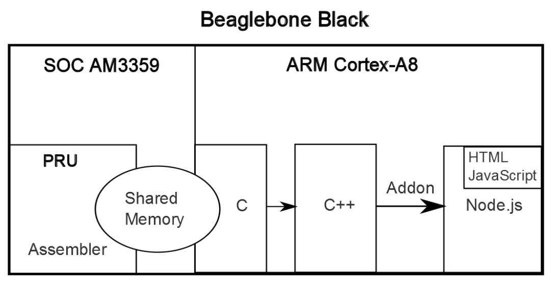
D.1. FPGA data to PRU
Generally, neither PRU nor FPGAs are developed to communicate with each other efficiently. They even use different languages in our design: the FPGA is programmed in VHDL, the PRU in C and assembler. Thus, interfacing the two can be a challenge. First of all, FPGAs do not have dedicated logic for communicating with PRUs or microcontrollers. So a suitable logic module must be designed from scratch. Secondly, the communication between the PRU and FPGA is asynchronous. So special care is needed to resynchronize the PRU to the FPGA clock domain. Finally, there is an issue of bottlenecks, both at the interface and on the PRU bus. Transferring information between the PRU and the FPGA usually requires cycles on the PRU bus and usually ties up the resource (PIO) used to effect the transfer.
Care must be taken to avoid bottlenecks with external RAM (if external RAM is needed). In our design, correct data transfer is guaranteed by a custom parallel communication link based on an 8-bit parallel data bus, and an enable, clock, and pause/start signal line. The PRU is programmed in assembler code and passes the data to the CPU with the help of shared RAM memory (The CPU
and PRUs both have access to the 8 KB data RAM0, 8 KB data RAM1 and 12 KB shared RAM). The PRU uses two 8 KB data buffers RAM0 and RAM1 alternatively to store the data from the FPGA. To enable the PRU, the Linux Device Tree (DT) should be configured firstly. The Device Tree (DT), and Device Tree Overlay are a way to describe hardware in a system. It describes the available pins, how specific pins should be muxed, and which driver to use. The original BeagleBone did not use a DT, but the recently released BeagleBone Black was released with a DT and is now using the 3.8
Linux Kernel.
The concrete realization of the protocol is referred to the file attached "PRU_source code.pdf"
An introduction to the Beaglebone Black's PRU can be found on our Github:
https://github.com/ADLab2020/beaglebone-black-PRU
D.2. C++ Addon for Node.js
Addons are dynamically linked shared objects. They can provide glue to C and C++ libraries. V8 JavaScript, a C++ library, is used for interfacing with JavaScript: creating objects, calling functions, etc. Documented mostly in the v8.h header file (deps/v8/include/v8.h in the Node source tree), which is also available online. In this step a C++ addon called addon.cpp is implemented to map the functions in C++ to Node.js,
D.3. Webserver Using Socket.IO Library
Socket.IO aims to make realtime apps possible in every browser and mobile device, blurring the differences between the different transport mechanisms. It is care-free realtime 100% in JavaScript. It has two parts: a client-side library that runs in the browser, and a server-side library for node.js. Both components have a nearly identical API. Like node.js, it is event-driven. By embedding the JavaScript for socket.io in the webpage (written in HTML) the users/clients can initialize the socket by just opening the webpage. After the initialization the users have full control over the front-end oscilloscope. To alleviate webserver’s burdens only the Canvas 2 on the webpage gets regularly updated with newly incoming data from the front-end.
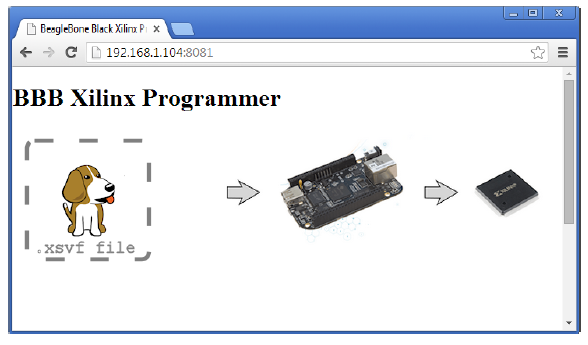
D.4. Program FPGA via Beaglebone Black
It is browser-based and simple to use with drag-and-drop programming. Just drag your programming file from the desktop onto the beagle in the browser. no menu or CLI at all. It takes just a few seconds to program a small FPGA like the Spartan-6 lx9. FPGAs have a JTAG interface and the BBB runs some software that can take a programming file (*.xsvf) and sends it over some I/O pins that are connected to the JTAG interface of target device. The web interface makes use of Node.js.
The real-time oscilloscope demo can be found on our Youtube channel:
https://www.youtube.com/watch?v=b4dWjJkLuDY&t=1s
****************************************************************************************************************
****************************************************************************************************************
Part - II Equivalent-Time Sampling Head
The general need for sampling systems is caused by the normal gain-bandwidth limitations of amplifiers. The realtime oscilloscope is limited to a bandwidth of 100 MHz. This sampling head serves its purpose to address these limitations and confer the Etherscope the capability of handling
high frequency repetitive signals. This block diagram shows more details about the design of our sampling head. It mainly contains two parts: trigger circuits above and S/H (Sample & Hold) circuits below.
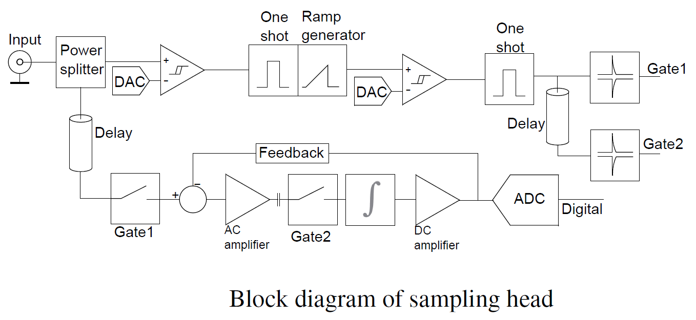
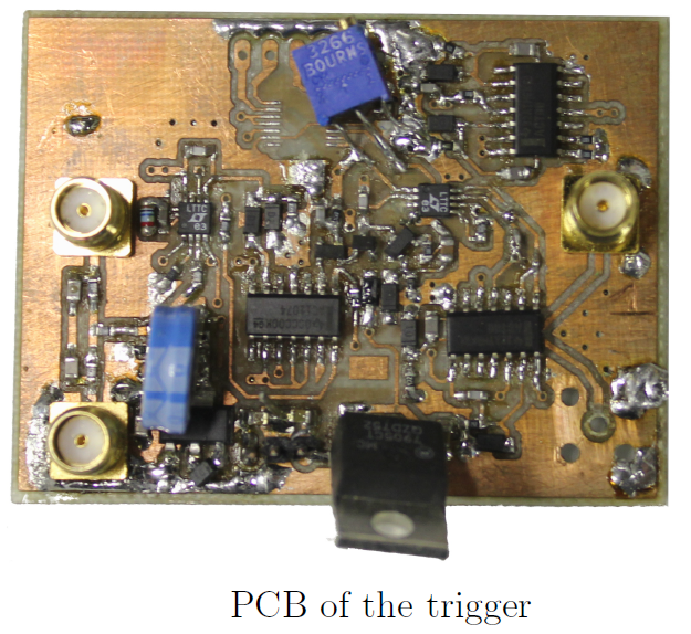
A. Trigger Circuit
The input signal is unequally split in two parts. A small part of power goes into the trigger circuit, generating a one shot trigger pulse by a first comparator. The trigger pulse initiates a sawtooth wave or a fast linear ramp by discharging a capacitor. By adjusting the second DAC, the time delay between the trigger pulse and the output pulse of a second comparator can be set accurately. This second pulse is referred to as delayed trigger pulse. It is reshaped to form the sampling pulses which can open and close the sampling gates. Especially the sampling pulses for gate 1 are very critical. After a fixed extra delay, the delayed trigger pulse is reshaped for driving the memory gate (gate 2), for which the pulses are much less critical.
B. Sampling pulses
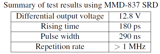
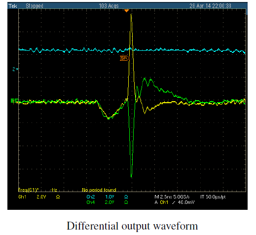
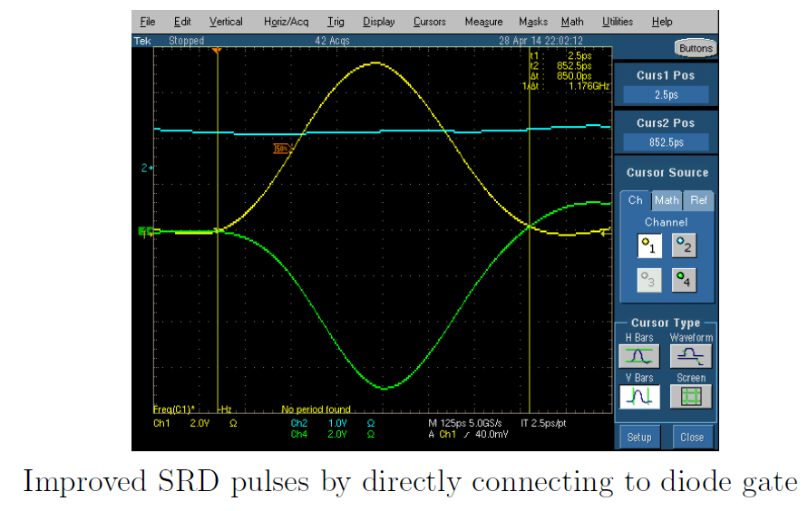
In order to open or close the sampling gate (1st gate) ultrashort and wideband pulses are indispensable. The essential principle of generating ultra-wideband pulses is charge-storage and discharging with a input trigger signal. Special solid-state components are utilized as the pulse sharpeners such as avalanche transistor, step recovery diode (SRD), tunnel diode etc. Our design requires the pulses to fulfill the following specifications: 8V, 50 impedance matching, 200ps pulse width and up to MHz repetition rate.
C. Sample and hold
A sequential sampling approach is adopted in our design. In other words, the trigger level set by the second DAC is increased progressively, forming a slow ramp. For each and every trigger point of the second comparator, multiple samples are taken to bring the feedback loop in a new steady state. And once the loop output voltage is stable, the ADC output values are suitable for further processing. The number of samples needed for one such acquisition depends i.a. on the loop parameters feedforward gain and feedback attenuation. The number of samples taken per unit equivalent time is dependent of the repetition rate of the input signal and the hold-off time of the system.
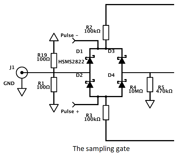
At a precisely timed repetition rate, and during a very short time interval, a switch is opened to measure the signal voltage. This switch is called the sampling gate. There are plenty of sampling gate circuits (single diode, double diode, balanced and unbalanced, CMOS, etc,) but not many that are fast and accurate enough for our purpose. Our design employs a diode bridge as sampling gate. The balanced structure implies that the differential sampling pulses are cancelled out when the sampling pulses and bias voltages are perfectly symmetrical. In this case there will be no sampling pulse left at the input and output and the leakage of the sampling gate can be largely reduced. The symmetry also suppresses common mode noise occurring in both sample pulses. This way, the SNR
(Signal-to-noise ratio) of the sampling gate is also enhanced. At a precisely timed repetition rate, and during a very short time interval, a switch is opened to measure the signal voltage. This switch is called the sampling gate. There are plenty of sampling gate circuits (single diode, double diode, balanced and unbalanced, CMOS, etc,) but not many that are fast and accurate enough for our purpose. Our design employs a diode bridge as sampling gate. The balanced structure implies that the differential sampling pulses are cancelled out when the sampling pulses and bias voltages are perfectly symmetrical. In this case there will be no sampling pulse left at the input and output and the leakage of the sampling gate can be largely reduced. The symmetry also suppresses common mode noise occurring in both sample pulses. This way, the SNR (Signal-to-noise ratio) of the sampling gate is also enhanced.
The sampling oscilloscope demo can be found on our Youtube channel: