 zpekic
SIFC16 CPU instructions - unlike on most processors - do not have any address mode specifiers, or fields. Yet, 5 distinct address modes are supported:
- Immediate, M[IMM] (or M[P+])
- Indirect M[X], M[Y], M[S]
- Indexed with base M[X+Y], M[P+X] etc...
- Stack M[PUSH], M[POP]
- Register implied (INX, SRC, DEY, etc.)
How does this happen? The address generation logic happens through purely combinatorial logic driven by operations on the registers.
In following simplified diagram, names of signals are same like in the implementation code for easier reference. Let's trace the memory address bus signals backwards, to their origin!
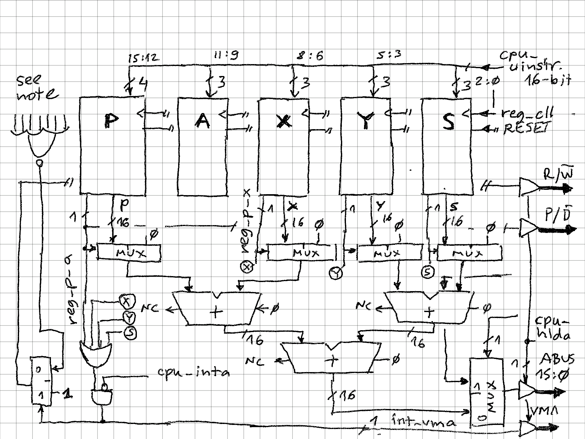
ABUS - tri-state output, 16-bit
This is usual, non-multiplexed address bus, able to address 64k words of memory. I/O devices are also memory mapped, MOS65xx or MC68xx style. The bus is tri-stated with cpu_hlda signal, which is generated by the control unit as a response to HOLD external DMA signal.
The raw address is generated by two sources:
- cpu_upc (microcode address) in case processor is executing trace sequence (that way external circuit can know which internal register DBUS is presenting). During trace sequence, cpu_bctrl signal is low which disables the VMA (valid memory address) signal.
- Register value sum (when cpu_bctrl = 1, which is normal operation). P, X, Y, S registers are able to contribute to this sum, but not F or A.
The register opcode itself determines if it will contribute to the address or not. This is done by driving the reg_?_a signal. This signal then either gates the register output value to be 0 (to not sum) or allows it, so it is added. For example register S (stack pointer) will drive this signal to 1 for M[S], M[POP], M[PUSH] only, but not the other 5 operations it supports:
-- projecting as address
with operation select reg_a <=
	'1' when r_s_M_POP,
	'1' when r_s_M_PUSH,
	'1' when r_s_M_S,
	'0' when others;
Other registers (X, Y, P) have similar logic (in reality just a 8 to 1 MUX with hard coded inputs!). It is now easy to see how M[X], M[Y] will be interpreted as base + index address mode, as both register values will be sent through the adder circuit.
VMA - tri-state output, 1 bit
Valid Memory Address signal is tri-stated also by cpu_hlda. Beyond that it is generated by simple combinatorial logic:
- if CPU is in interrupt vector read cycle, it will be 0 (interrupt vector is expected on DBUS not any memory location value)
- if CPU is not in interrupt vector read cycle, if ANY register projects address (reg_?_a is 1) then VMA will be 1 too.
RnW - tri-state output, 1 bit
This is a Read (1) / Write (0) signal. Tri-stated by cpu_hlda as expected. But origin is a bit more complicated:
- If VMA = 0, then it is always "Read" (1) - except in the case of tracing (output of register values, this is not represented in the diagram above due to mistake)
- if VMA = 1, it is "0" (Write) when at least 1 register is projecting data (for example STA projects data, but SRC does not). This is indicated with the NOR gate with 7 inputs. 5 of these are connected to P, A, X, Y, S registers (reg_?_d outputs) and 2 are detecting FTOS and PUSHF instructions when F register is to be written to memory.
PnD - tri-state output, 1 bit
Program (1), Data (0) - this optional signal can be used to allow implementation of "Harvard" system with program and data memory split (64k words each). It is simply connected (through usual cpu_hlda tri-state) to reg_p_a signal generated by P (program counter) register. If 1, it means that P is involved in address generation, so the address is either program code, or data stored in the program memory (for example M[P+X] lookup etc.).P is projecting address in 11 opcodes, out of 16:
-- projecting as address
with operation select reg_a <=
		'0' when r_p_NOP,
		'0' when r_p_LDP,
		'0' when r_p_STP2,
		'0' when r_p_STP4,
		'0' when r_p_STP,
		'1' when others;
Discussions
Become a Hackaday.io Member
Create an account to leave a comment. Already have an account? Log In.