 zpekic
CPU internal data paths come in many topologies and complexities - from simple bidirectional bus all the way to n*m matrix switches and everything in between.
SIFC16 datapath mostly resembles a circle, in the sense that outputs of all registers end up as inputs of these same registers:
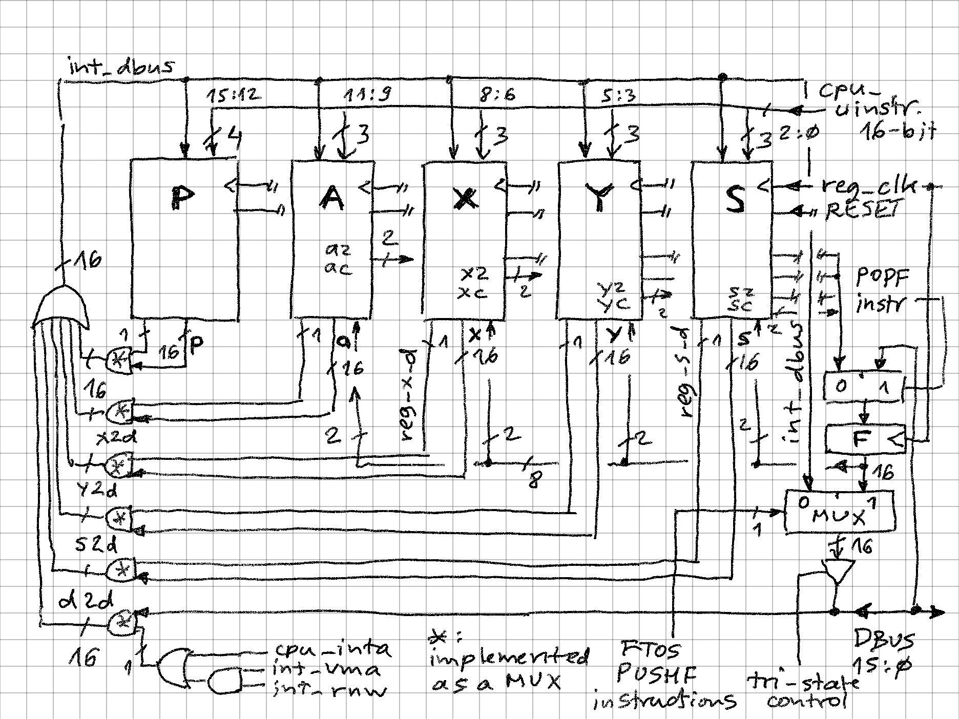
There are also a few side loops along the way (for external data bus and F (flag register). Signal names are same like in the implementation, for easier following.
Reading data (from registers or memory)
Each of the registers (P, A, X, Y, S) generates two signals:
- 1-bit data output enable, which depends on the operation
- 16-bit data (register value)
For example index register X (and Y):
-- value
reg <= r;

-- projecting as data
reg_d <= '1' when (operation = r_x_STX) else '0';
So if reg_x_d is 1 (in case of STX or STY operations), then then "and" gate (which is actually a 32 to 16 MUX) will pass the value along to be combined in a OR gate array (16 OR gates, each 6 inputs wide, seen on center left):
- 5 inputs of the OR array are gated register values
- 6th input comes from DBUS (memory data bus). This input source is passed through if:
- interrupt vector is being read (cpu_intr control signal) - OR -
- memory address is valid (VMA = 1) and "read" mode (RnW = 1)
The combinatorial logic above drives the 16-bit internal data bus (int_dbus) which is then fed back to each register.
Here are some examples how this works out:
LDA, STX, STY;
This is A <= X or Y, because both X and Y are projecting data, which will be OR'd and A is loading on next rising clock so it will load that value from internal data bus.
LDX, M[POP];
This is a POPX (pop X from stack). S is projecting address, so VMA will be 1, but because no register is writing, RnW = 1, so DBUS will be passed through to the OR gate array to drive int_dbus. This value will be loaded in X register on next reg_clk rising edge.
Writing data (from registers)
Values gathered through OR gate array and present on int_dbus are circled back towards a MUX that drives DBUS through a tri-state gate (cpu_hold combined with RnW signal). If VMA = 1, and RnW = 0 (see address generation log entry for explanation how this happens), it means that values from registers can be written to memory. For example:
SRC, STX, M[S];
X is written to stack top memory - A does not generate "project data" only internal operation so it won't be present in the internal data bus, but X will be, and because of that RnW will be 0 (Write). S "projects address", so VMA = 1.
M[X];
Valid, but useless instruction (effectively a NOP) - no register "projects data" so RnW = 1, X register "projects address" so there will be a valid memory read, and internal data bus will carry the value of memory location at address X, but no register will load it.
Writing F (flags)
F register can only be written to memory, and only using stack operations. Two special instruction combinations allow this:
constant c_FTOS: std_logic_vector(15 downto 0)     :=    r_p_NOP & r_a_NOA & r_x_NOX & r_y_NOY & r_s_M_S;        -- mostly for flag output in trace mode
constant c_PUSHF: std_logic_vector(15 downto 0) := r_p_NOP & r_a_NOA & r_x_NOX & r_y_NOY & r_s_M_PUSH;    -- flags to stack
When these combinations are detected (simple combinatorial match of the 16-bit instruction word), then the MUX in bottom right corner would flip the input to the F side, so F register would be written to DBUS (VMA = 1 because S "projects address", and RnW = 0 as explained in the address log)
Reading F (flags)
F register - just like all the others - is updated on EVERY rising edge of reg_clk. To avoid losing the flag values, in almost all cases this means every flag bit makes a full round trip through its register. For example ac and az (accumulator carry and zero flags):
-- zero flag output
with operation select zo <=
      zi when r_a_NOA,
      zi when r_a_STA,
      y_z when others;

-- carry flag output
with operation select co <=
      y(17) when r_a_ADC,
      y(17) when r_a_SLC,
      y(0) when r_a_SRC,
      ci when others;
It is obvious that unless the operation affects the flag (shift, load, add), the output is same as input. In other words, flags will be unaffected. But other extreme is true too:
XOR, CPX, CPY, CPS, M[IMM];
.data 0;
This instruction will simultaneously update 7 flags: az, xc, xz, yc, yz, sc, sz (XOR only affects Z flag, but CoMPare affects Z and C because it is a binary subtraction with discarded result).
The only case when this flag circular data path is broken is in case of the POPF instruction:
constant c_POPF: std_logic_vector(15 downto 0) := r_p_NOP & r_a_NOA & r_x_NOX & r_y_NOY & r_s_M_POP; -- pick up flags from stack
When this 16-bit instruction pattern is detected, the F input MUX will flip on the DBUS side. Because S is "projecting address" VMA will be 1, and RnW will be in default state 1 ("read"), so F will be picked up from stack. F register can only be loaded / saved through the stack, not directly from any other internal register.
In summary, this design has some advantageous features:
- Orderly implementation of registers - all have same "interface" of 1 data input, 1 data output, 2 flag inputs, 2 flag outputs etc. (with exception of P and F). Critical for the design are 2 control outputs per register:
- reg_?_d - 1 when output is to be interpreted as data ("project data")
- reg_?_a - 1 when output is to be interpreted as address ("project address")
- Single clock, single clock domain drives all the registers and control unit (no phased or delayed clocks etc.)
- Predictable and short delay times (only 2 gates between register output and register input)
Discussions
Become a Hackaday.io Member
Create an account to leave a comment. Already have an account? Log In.