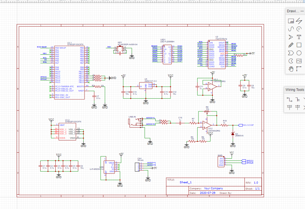
Features:
1 Based on STM32F103C8T6, sufficient performance space is reserved to facilitate the expansion of functions in the future
2 Red 2088B lattice, driven by MAX7219, easy to program
3 Standard 3.5mm audio interface, powered by USB.
4 An integrated power supply/audio interface is reserved for further DIY
5 Spectrum analysis and display based on FFT, non-level display
6 The gain can be adjusted to accommodate small signals
7 Flip through the button display, convenient to switch the position of the audio interface left and right.
Notes for welding and use:
1 J1 and J2 jumpers are used to choose whether the input signal is left channel signal or right channel signal.
2 The input voltage should not be higher than 5.5V.
3 The R8 on the board is used to adjust the gain. The maximum gain is 10.
Schematic File Designed by EasyEDA , a free online PCB software
PCB Prototype Manufactured by JLCPCB by $2 for 5 pcs
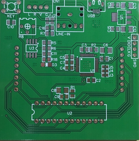
PCB Design File
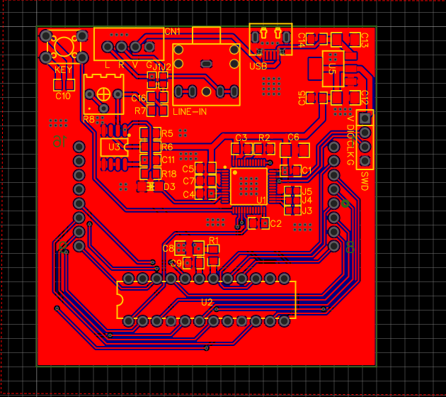
The BOM list also enclosed for reference.

 MSchmidl
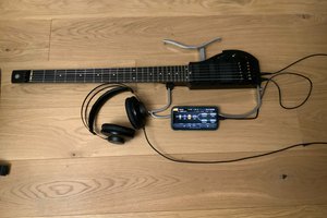
 courcirc8
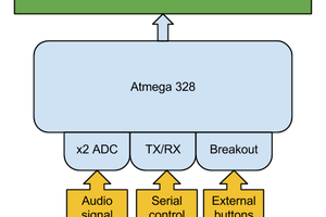
 CrazyChip
 mircemk