 John Duffy
The schematics are done! I kind of want to do a video going over the design process as this has evolved over what's now several years, there have been a ton of changes to everything.
For now I'll throw some (slightly) better explanations here.
Lets get right into it.
Overall block diagram below. Nothing too surprising, we've got our Volts, Amps and Ohms sections (AFE = Analog Front End) separated, a PGA (programmable gain amplifier) and ADC, and microcontroller. Specifics of the interconnects to the MCU aren't super important, mostly just some control outputs to the subsections and digital connections to the PGA and ADC. Only real thing of note is that the front Common jack DOESN'T go straight to the COM global label (which is generally used as our common in the subsections) - it takes a detour through the Amp AFE first. It doesn't affect much but we'll come back to it.
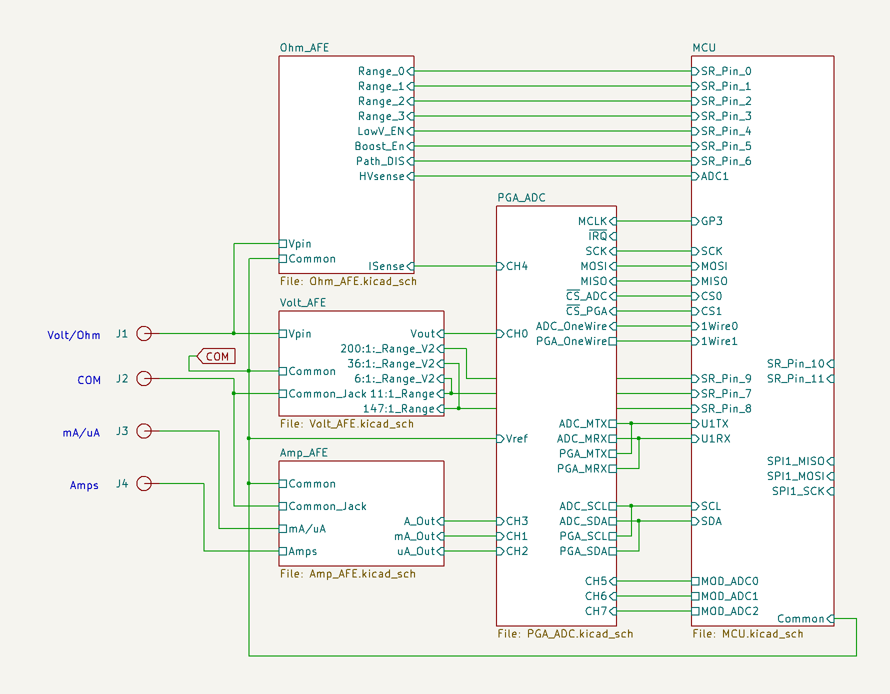
Few things to note in the analog sections are that there are a few different power/signal rails, COM is the star of the show, it's our reference voltage, everything else will be measured relative to that. It's the same voltage as the Common Jack on the front of the meter.
If you're familiar with splitting a single power supply for a virtual ground, skip this paragraph. If not I won't go through it in a ton of deail, upshot is that COM is about 1.65V (half of 3.3V) relative to the power supply 0V. It's driven by an opamp (caps are just for decoupling, only R52 and R51 matter):
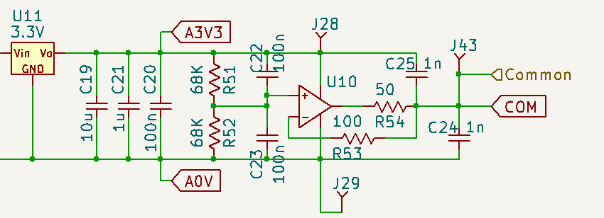
(this wasn't big enough for it's own section so it's in the MCU section, same as the other supply stuff).
Battery- goes to "D0V" (Digital 0 Volts), Battery+ goes through a 5V regulator to "VSYS". So VSYS is at 5V relative to D0V. The pi pico regulator creates "D3V3" (Digital 3.3V, relative to D0V, used to power digital stuff) from VSYS. "A0V" (Analog 0 Volts ) is connected through a choke to D0V, and U11 shown above creates "A3V3" (Analog 3.3 Volts) relative to that, which is used to power analog parts like opamps. So A0V ~= D0V (but hopefully without some of the noise), and A3V3 is 3.3V relative to A0V, so ~= D3V3 but may be up to a couple hundred mV apart depending on the regulators. COM is halfway between A3V3 and A0V, so is roughly +1.65V relative to A0V.
Upshot: split rails, A0V == D0V = 0V, COM is middle, A3V3==D3V3 = 3.3V COM ~= Common Jack, but only for low currents
We'll start with the Voltage section since it's pretty straightforward. I made a different version of this as well with a constant input impedance (10MΩ), while this one varies between 10MΩ at < +-1.5V and ~1MΩ at higher voltages. I'll go into that version later, it's more complicated and not sure it's going to work, while I've already tested this one.
The basic parts are the inputs (Vpin) which goes directly to the front jack, same as Common_Jack, Common, which our reference voltage ("ground"), the protection resistors, R1-R10 (which total to 1MΩ), the attenuation resistors R13 and R14, two switches in U1, "Vout" which goes to the ADC, protection MOVs/GDT, and the frequency compensation caps. All U1 does is switch R13 or R14 (or neither), and their associated caps, to common. If we ignore the caps for now, this causes the node at Vout to be the center tap of a voltage divider, with R1-R10 (1MΩ) on the high side, and either R13 (100KΩ) or R14 (6.8KΩ), in parallel with R12 (9.1MΩ), on the low side.
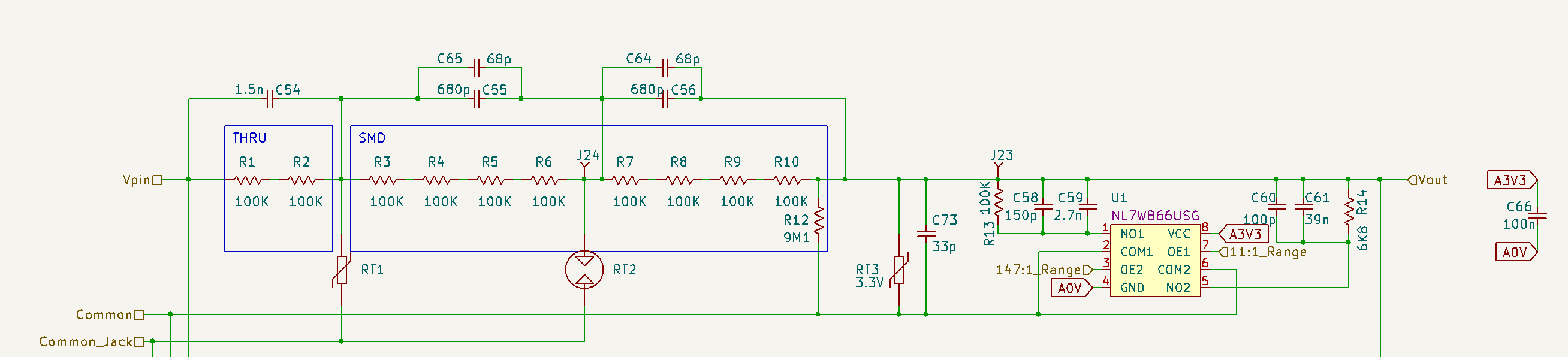
This gives attenuation values of ~1.11 : 1 for neither resistor (and a 10MΩ input impedance), ~11.1 : 1 for R13, (and a 1MΩ impedance), and ~148:1 for R14. The ADC can take voltage from A0V to A3V3, so about +-1.65V relative to COM. To keep from nonlinearity near the rails, we'll limit to about +-1.5V relative to COM, this sets our three voltage ranges to 1.5*attenuation ratio, or about +- 1.7V, 17V, and 220V.
Note that while technically that last range means AFE should be able to handle it, this is NOT meant to measure anything outside of low voltage DC. I want to get some experience with dealing with front ends designed for this sort of thing and learn what sorts of problems come up, I'm sure there's some horrendous flaw in the design that will get someone killed if they build this and try to measure mains. If you have experience with this sort of thing, do let me know how exactly I messed up :).
The input resistors are split up like that, instead of a single big 1MΩ resistor, for input protection. This way I can gradually step down any overvoltages, with more resilient but less precise components up front, diminishing the fault as it moves to the right until very small parts can handle it without interfering with normal operation outside of a fault. R1 and R2 are larger through-hole resistors which should be able to withstand some higher voltage and abuse, and can be mounted for a very large creepage distance. RT1 is a 230V nominal varistor, which should clamp any overvoltage to about 400V at the node above it. So say we have 10KV at the input, RT1 will conduct with a voltage drop of about 400V, so well have 9600V across 200K, which should pass about 48mA. Most of that will go through RT1 and back out the common jack. For a very short pulse, this *should* be fine, way exceeds the power rating of everything but if it's only a few uS they shouldn't have time to heat up. This is also why we separate COM and Common Jack somewhat, while connected elsewhere (in the amp section) - higher currents in fault conditions should avoid passing through any of the more sensitive parts. So we've now got ~400V across RT1. R3-R6 are 400KΩ together, and RT2 has a glow voltage of about 75V and up to 10mA (won't dive into GDTs right now, they also have an arc condition but that doesn't come up in this example), so we should see a little under 1mA going through it, and 75V at the node at J24. Finally we've got another 400K, and RT3, which should limit us to about 175uA to COM, which RT3 can limit to just ~5V, from there R13 and R14 plus the input protection diodes can protect the inputs to U1. So we've handled 10KV at the input without damaging anything OR dead shorting the input and allowing high current flow (important for avoiding arc flash!), as long as it doesn't last too long.
At least that's the idea/rationale for everything, no idea what will fail in practice (I'm sure there's things I don't know here, so something would go wrong, part of this project is learning what some of those are, and how to do it right!).
Finally all the capacitors are to keep everything working at higher frequencies, since all our nodes are pretty high impedance, a few pF of capacitance to ground will start to form an RC circuit (most notably, the big MOV, RT1 has about 70pF). If we form a capacitive divider with the same ratios as the voltage dividers though, this effect goes away and the circuit can pass higher frequencies, and with the correct attenuation when switched.
Whew that was a lot. Moving on to the Amps section. Bonus we finally get to get this whole COM vs Common Jack thing sorted out.
Well *that's* a lot simpler.
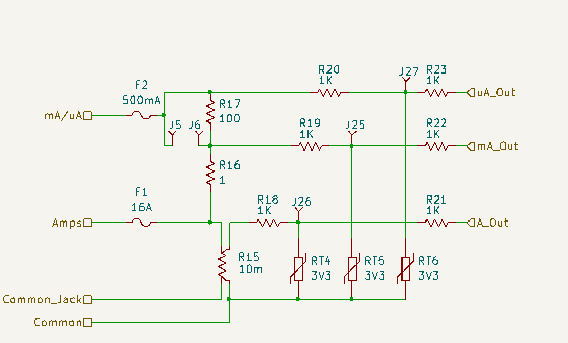
We'll start with the ~10 Amp range. Current comes in the front panel jack ("Amps" label) goes straight through a fuse, through R15 which is a 4-terminal shunt resistor, and straight back out the Common Jack. To avoid having voltage drop in the board traces at higher currents throw off the readings, we use a "4-terminal" resistor. Really it's a 2-terminal resistor because they're cheaper, but we're setting up the footprint specially to force some small sense taps right at it. This is where COM comes from - so it IS wired straight through to Common Jack, BUT has these smaller low-current traces and may have some voltage drop relative to it. So, we force it to be connected at only this one point to avoid ground loops and measure only the resistor. This also means fault currents passing to ground out of the Volt AFE can only go straight back to the Common Jack itself, not through other stuff where it might hit a thin trace and cause problems. During normal operation, there will be very very little current flowing from COM in/out of the jack, so they'll be at basically the same voltage.
mA and uA are similar but have larger shunts, R16 and R17, J5 and J6 are wired to a mechanical switch to switch between ranges. Not much else to write home about here, the resistors on the right offer the same kind of input protection to the ADC (uA_Out, mA_Out, and A_Out go straight to the PGA/ADC). Since we're shunting power to ground through the R's and have the fuses already, and there's no actives at all, we don't need much in the way of fancy protection. I may want to add some diodes to limit the maximum burden voltage on the uA range, but have to start worrying about leakage and stuff and it's just another part to add. May be a problem if it's like, put across mains in uA range, but not super worried about that particular situation.
Ohms!
Oh ohms.
This part was the biggest pain in the ... patootie.
Biggest things I wanted out of this that made it hard was
a) Optimizing every part out of it that I could - I wanted this as simple as possible. In the end I got it down to 6 transistors and one opamp
b) Diode test should be at least +3.6V, for white and blue LEDs
c) No separate ohms jack, has to be a single port like most regular multimeters
d) Some level of input protection. Not expecting this to be bulletproof, but should have some chance of surviving high voltage on the port
e) The range of values we have to cover, from single-digit ohms to megaohms - so >6 orders of magnitude of resistance all have to be accounted for
Basic theory of operation is, obviously, based around Ohms law, inject a known current through the resistor we're testing (which I'll shorten to DUT: Device Under Test), and measure the voltage across it. So the Ohms section is just responsible for sending a known current out of the voltage jack, and then we use the regular voltage AFE to measure, well, voltage.
This went through MANY iterations, all around one of two basic ideas. The initial idea was to have a full high-side current source, set by a logarithmic DAC. This was possible but added a lot of complexity and cost, many opamps to do ranging, level shifting, feedback, and measurement. The way I settled on was to just switch one of 4 resistors to the upper rail and measure the voltage drop across is (and thus, current though it). One big change that simplified things a lot was separating the input protection for ohms from the voltage section entirely, originally I had some resistors and a PTC common to both paths, which would be added to the DUT, so any significant resistance or a PTC would make it impossible to measure small values. At some point I realized that if I think about it like a kelvin/4-wire/remote sense terminal at the voltage jack, with completely separate protection paths for volts and the current source, then I can completely ignore the input protection, while it will have some voltage drop from the current source, as long as it doesn't sink any current to ground, it will be the same amount of current going out the jack. The final design for this uses a bank of 4 resistors, from 500 ohms to 1M with a pfet connecting each to a ~9V positive rail (made by a boost regulator), and the other end connected, through the input protection, to the voltage jack. By measuring the voltage drop across that resistor and knowing its resistance, we know the current through it. Knowing that that current is also going through the DUT, and measuring the voltage across the DUT using the regular voltage frontend, we can compute the resistance.

This circuit has three different "flows" (current out, current measurement, and protection), so it's not quite left-right like most schematics. Current out flows top down to Q1, then left out of Vpin, measurement goes from the FET/resistor array to the right through U4 and out at Isense, and protection "flows" from Vpin in through up to Q1, and down to the section at the bottom. Little weird but this kind of made the most sense in my head.
At the top we can see the isolated boost regulator (U6) to make ~9V. Q12 is just to switch it on and off so it doesn't draw power when we're not in ohms/diode mode. This puts about 9.5V relative to COM at the "9V5_Ohms" node. Because it's an isolated regulator, even through we're drawing power from the D3V3-D0V rails, we can have the return path be to COM, so we're not pushing any of this current back into the opamp that generates COM. If we did it could cause noise on the rail or pull it around as current is drawn. We only ever source about 5mA, so the opamp *should* be able to hold it, but still best not to.
D2 drops the 9V5 by a little bit before getting into the shunt resistors, so the positive rail for the opamp (U4) can be a little higher than its inputs will ever be. It is a "rail-to-rail" opamp so hypothetically it'd be fine not to, but this gives us a little breathing room and avoids any weird nonlinearity or loss of performance *right* near the rail. We'll get back to U4 in a second.
From the cathode side of D2, we get to the rail we use for everything else. One of the 4 P-Fets, Q2-Q5, are turned on to enable a specific range, set by the resistor at its drain, R26-R29. R26 for the <1K range, up to R29 for the >~300K range. Q7 through Q11 and the other resistors around there are just to allow the microcontroller to switch the gates of the fets, which have to sit at about the 9V rail to be off.
From there we tap off the voltage at the low side of the range resistor and send it to U4 to measure the voltage across the resistor. We'll get to that in a second what matters for now is that (effectively) no current flows that way, it all goes down to Q1. We will... also get back to Q1 in a second, for not assume it's just all the way on and passes the current down. Since the gate on a fet (effectively) draws no current, all the current flows down to the node at J16. D6 is reverse biased, and RT7 is a MOV that's under it's minimum varistor voltage, so neither draw any current, so it all passes to U5. U5 is a solid state relay, again assume it's on, so all the current passes through to D1, F3, and R25, this stage is all input protection. Ignore the wire heading down, and finally J7 and J8 have a switch between them to connect this circuitry to the voltage jack (Vpin)! Finally.
Finally getting back to U4. So the current is measured by the voltage across whichever shunt resistor (R26-29) is selected. Voltage is measured across both the Pfet and resistor, so from the net with J13 to the one with J15. Since the RdsOn of the fets is really low, it doesn't contribute significantly so we can assume we're pretty much just measuring voltage across the resistor. What we're looking to do is measure this differential voltage without drawing current from J15, and output that relative to COM, somewhere within the range of +-1.5V. Note that while the J13 net is relatively low impedance, the J15 net may have an impedance up to 1 Meg, and since we're counting on all the current from the resistors going through the DUT, we can't draw any current from it anyway. This means a normal differential opamp circuit is out, the resistors used would draw current from the net. What we'll do is convert the differential voltage to a proportional current (being sourced from the high voltage rail), and sink that through a resistor going to COM, converting it back to a voltage, relative to COM.
To accomplish this, the J15 net, goes directly to the + side of the opamp, U4. Basic opamp circuit, long as the feedback is set up correctly, this will drive the - terminal to the same voltage as +, so we can assume it is at the same voltage as J15. Notice then that R30 is connected between opamp - and J13, so it has the same voltage across it as the shunt resistor. Thus, it will have a current through it proportional to that voltage. To keep this current from just being sunk into the opamp, we put another pfet (Q6) with its gate to the opamp output, which means that while the opamp can control the current through R30 by keeping Q6 in its linear region, all that current ends up at the drain of Q6 - hey presto, this forms that voltage controlled current source we said we wanted a second ago! Finally that current goes through R31, and we've got our sense voltage. By setting the ratio of R30 to R31, we can set the ratio of that output to the input voltage as well, in this case 3.3:1 - this means that with the ~1.5V range of the ADC, we can measure a shunt voltage of up to ~5V.
The only real disadvantage to this is that the sum of voltages across R30 and R31 can never exceed the supply voltage - about 9V (plus we need some overhead for the pfet to have room to work). So for example if we have a shunt voltage (J13-J15) of say 7.7V (so sourcing 7.7uA to Vpin if we've selected R29, 1M range), then R30 *should* have 7.7V across it, which means R31 *should* have ~2.3V across it (=7.7 / 3.3, ignore that that's out of the ADC range for now). 7.7V+2.3V = 10V though, and we've only got a 9V supply! So that can't happen, what happens instead is the opamp turns Q6 all the way on, effectively forming a voltage divider of R30 and R31, which gives us about 2.1V across R31 and 6.9V across R30 - so we're no longer measuring current accurately!
The way this can happen is if our DUT is very small relative to the shunt resistor, worst case would be a dead short when we've selected the 1M shunt, R29. If this happens, R25 will only drop a couple mV, and since we're only sourcing ~9uA, D1 will only drop 0.2~0.3V or so so J13 is basically going to be at 0.2 or 0.3V relative to COM, so J13-J15 ~=8.7V, way too much. The way we fix this is having a couple volt drop in that path, if we have *something* (hint: it's Q1) that has a voltage drop of say 4V, then while the net with J16 might be at ~0.3V, J15 will be at 4.3V, so J13-J15 is only 4.7V, perfect! We could do this with something like a voltage reference, that would give very consistent drop, but we can get another benefit by using the fet. Note the numbers used there were pretty arbitrary, you wouldn't measure 0 ohms with that range, you'd use R26, but then R25 and D1 put it back in range, in reality it's values between ranges where we run into problems. This *could* be avoided by having like a dozen different ranges, but this kept a few parts off the BOM.
For low value DUTs, R25 is large enough relative to the shunt to drop enough voltage for this, so we don't need to drop any voltage in Q1, so we pull LowV_EN (which goes to a digital output pin on the microcontroller) low, pulling the gate of Q1 up to the rail, and turning it all the way on.
For higher ranges where R25 doesn't contribute much, LowV_EN is pulled high, turning on Q8, and forming a divider to hold the gate of Q1 at about 4.5V. Q1 is configured as a source follower, if you're familiar with these skip this paragraph, if not read on, uncommon enough use I figure I'll go through it. Basically the source is the output, the drain is connected towards the positive rail (in this case, our shunts). In an (almost) ideal FET, any voltage between source and gate turns it on, so if the source is pulled below the gate by some load (our DUT this case), it will turn on. Since the DUT has some resistance, the fet turning on will push current through it, increasing the voltage across the DUT, an thus raising the voltage of the source. Once the source gets up close to the gate voltage, it will start to turn back off, and sort of "balance" just below the gate voltage. This normally has the effect of buffering the gate voltage - since the fet can pass a ton of current from drain to source, we can source a ton of current from our positive rail to our load/DUT, controlled by the gate voltage but without drawing any current from it. In a real fet it takes some gate voltage to turn on, so it will balance at about that point below the gate. So, upshot is, if we hold the gate voltage at about 4.5V, and assume that Q1 has a Vgs of about 3V at the current we're passing, then it will keep the source at somewhere around 4.5V - 3V = 1.5V.
This actually solves two problems - one is getting some voltage drop, doing the math on the possible ranges and resistance values for the DUT (not going to go through that here this has already gone on FAR too long, exercise for the reader :) ) we can find that no matter what our DUT is, at least one of the ranges will both drop enough voltage across Q1 for the shunt sensing to work, and have the measured values be in a reasonable range, at least a couple hundred mV (in theory we could ignore all of this and just use the 1M shunt for everything, but then the voltage across a small DUT would be like, microvolts - difficult to measure accurately). The other problem this solves is the voltage going through the Volt AFE being over 1.5V - if it is we have to go to a higher range, which decreases the input impedance to ~1.1MΩ, which will be in parallel with our DUT. Not a problem for values less than a couple hundred KΩ, but towards the MΩ range, that's going to make it more difficult to get accurate readings. We will calibrate out the effect of the Volt AFE impedance, but that will simultaneously decrease our sensitivity to the DUT, AND force us to a higher range where the reading will be a smaller portion of the ADCs range, both hurting our accuracy. This source follower forces the output to be below about 1.5V, so we can stay in our 1:1 range, with 10MΩ input impedance! It's not super precise but is good enough.
Whew, that was a lot, but we've got all the parts on how this works. Imma put the picture again just so we don't have to keep scrolling up:
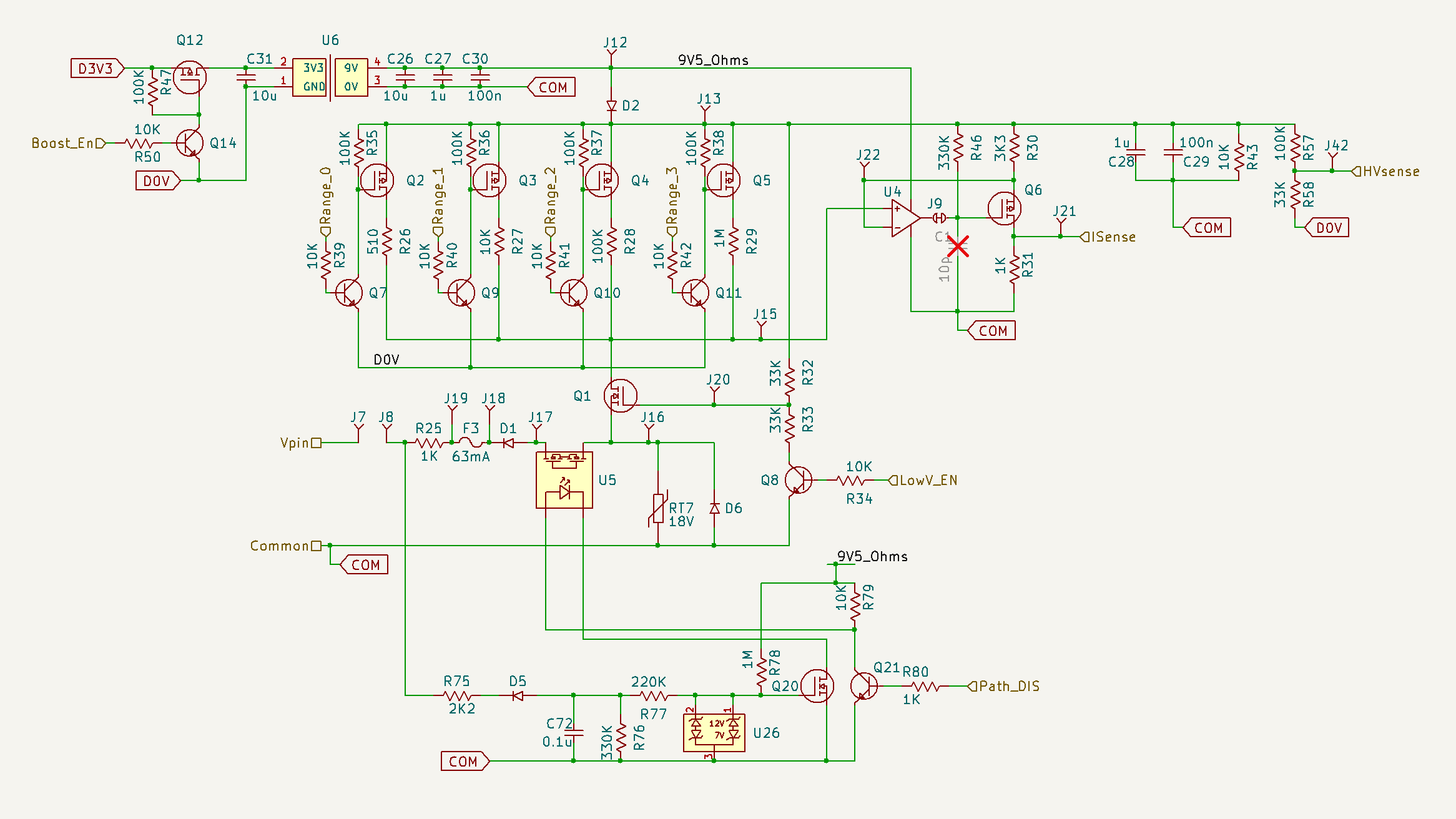
The couple passives to the right, C28 and C29 are just bypass caps for U4, R43 is there to load D2 so it's got at least ~0.5V drop, without that the load through our shunts will raise and lower it considerably based on the range and DUT. Doesn't really cause any big problems now but might cause some annoying problem down the line. This stabilizes it enough. Could use a ~8.5V linear reg or voltage reference instead of D2 to get even better stability and noise, but I'm not really worried about it. R57 and R58 form a voltage divider, HVsense goes to our micro's ADC, so it's got an idea what the J13 rail is sitting at. Won't be used for the actual ohms calculation but good to know to see if there's some error with it.
Last couple parts aren't super important for operation and are just protection. R25 is used just to limit any current from an overvoltage, it can't be ~1M like the voltage AFE so we can still source about 100mA/100V which isn't great (so plugging into mains would allow 170mA, probably enough to mess something up). F3 is obviously a fuse, we're never pushing more than about 5mA in normal operation so this should be more than enough to never trip unless we do something really bad. Finally D1 will keep any reasonable positive overvoltage from getting in. If we're seeing more than 1KV at the input ... yeah this thing was always going to blow up. RT18 and D6 limit any voltages that do get through, if we're at say the 1M range it won't take much leakage through D1, or big negative transient to pull this node otherwise. D6 will keep the rail from ever going below COM, which is the main concern here (that could potentially blow the gate on Q1). Finally U5 is used for negative overvoltage (which always feels a little weirdly mind bending to think about for some reason, really large, negative voltages...)
The lowermost section will keep the SSR's control LED on most of the time, but if there's a negative voltage at the input it will shut off, protecting the rest of the ohms section. R75 and D5 mirror R25 and D1, limiting the maximum current, and positive voltages. If we get a voltage below COM, C72 (which is a 1.6KV film cap, similar to the Volt AFE ones) will start to charge up. Time constant is only few uS, so D6 should be able to handle it for that time. That will go through R77 to the gate of Q20. During normal operation, R78 will pull the gate high, turning Q20 on and turning the SSR on. When a negative voltage comes through R77, it will pull this gate down towards or even below COM, shutting it off. U26 limits the voltage at the gate to +12 or -7V, so we can't blow up the gate. It's internal protection *should* be enough, but I'll put this in for now. If I'm really shooting to optimize the BOM I can probably cut this. There's a cap and stuff so that this will stay off for some time after a fault, C and R's are sized so it should stay off for a full power line cycle if connected to mains. Finally, if Path_DIS is brought high, it turns on Q21 and shorts out the SSR LED, turning it off. This can be used if we detect a fault and don't want to just rely on the undervoltage circuitry.
At some point I kind of want to make this a transistor based thing to cut cost down, that SSR isn't super cheap, but I already had a couple of them on hand and it simplifies things a bit.
FINALLY on to the next section, the MUX/PGA and ADC
Not a ton going on here, basically the MUX/PGA (U2) is an MCP6S28, which combines an 8 channel multiplexer and SPI-controlled programmable gain amplifier (PGA). For this and the ADC, I've got them mounted on breakout boards so they can be replaced with a different part in future if desired, to improve performance or add features or something. This is also why there's a bunch of additional test points nearby, they'll be placed next to the breakout board footprints in some standardized way (TBD), part of the modularity I was talking about way long ago. Minor note on the PGA, you'll notice J79 means its MISO pin isn't connected - this parts "SPI" isn't quite, it's essentially just a shift register that controls the channel and gain. So, MISO is low-Z even if CS is high, so it will interfere with the ADC. We don't need any data back from it, so it's fine to leave this floating. If I end up replacing this with some other part in future, a 0 ohm resistor or solder bridge on J79 will reconnect it.
ADC is an MCP3461R, a decent, 16 bit, fully differential ADC. One nice feature is it can run up to 1MSPS at 12 bit, which should let this have an "oscilloscope mode". It won't be very good but in a ton of cases I'm measuring something that's oscillating or browning out or something and a meter just isn't fast enough and I don't want to go take this to the bench (or a scope into the field!) - just being able to see a simple waveform on my meter would be a godsend. I know scopemeters exist but they're expensive and designed around being an oscilloscope that's portable, rather than a meter that can kind of act like a scope in a pinch.
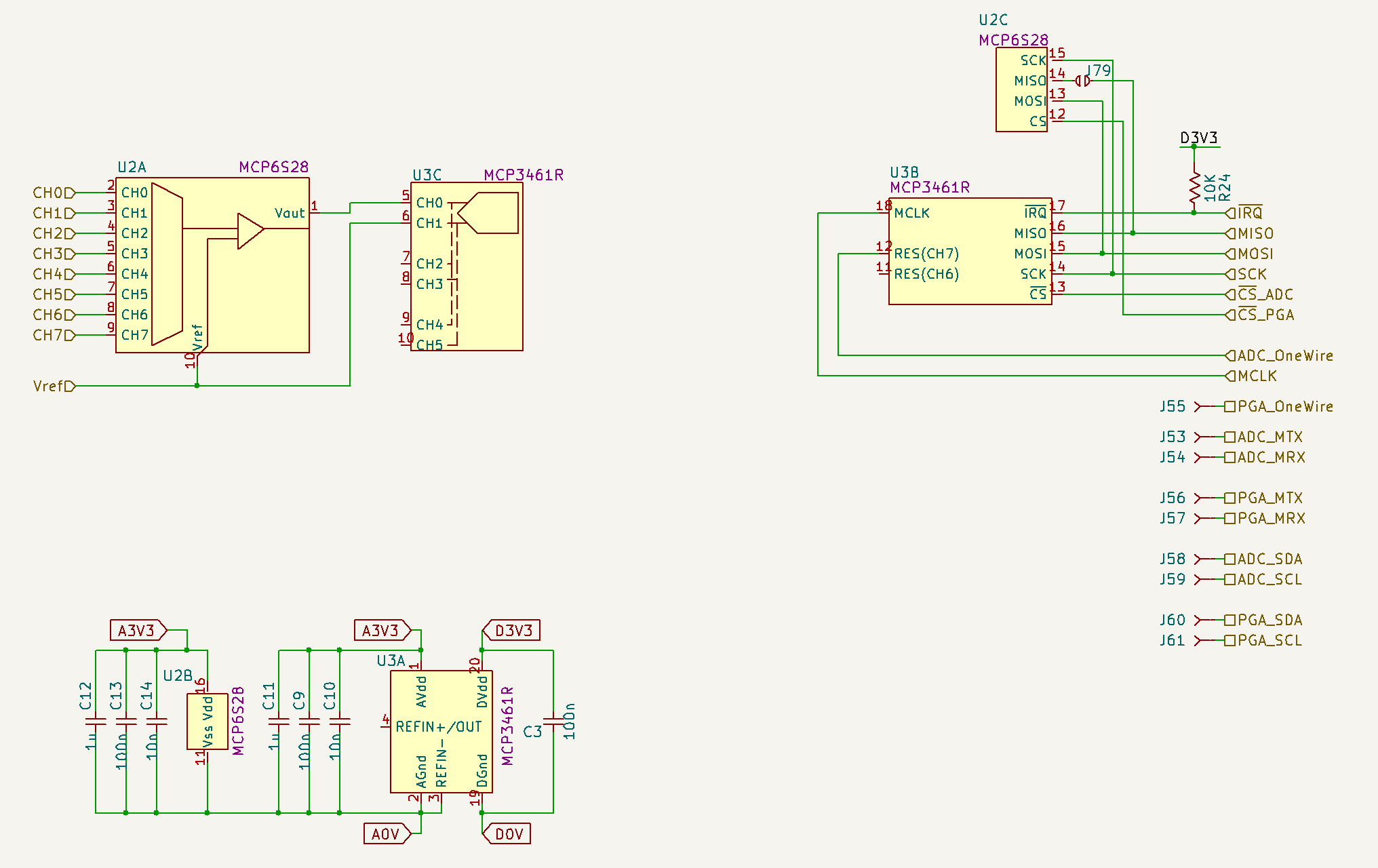
One thing that I want to make as standard as possible is having a 1-wire or I2C EEPROM on all the modules to identify them so they can be swapped without changing the MCU firmware. That's well down the road but adding connections for it now.
Last part is labeled the MCU section but has a couple assorted, related things that don't really need a separate sheet:
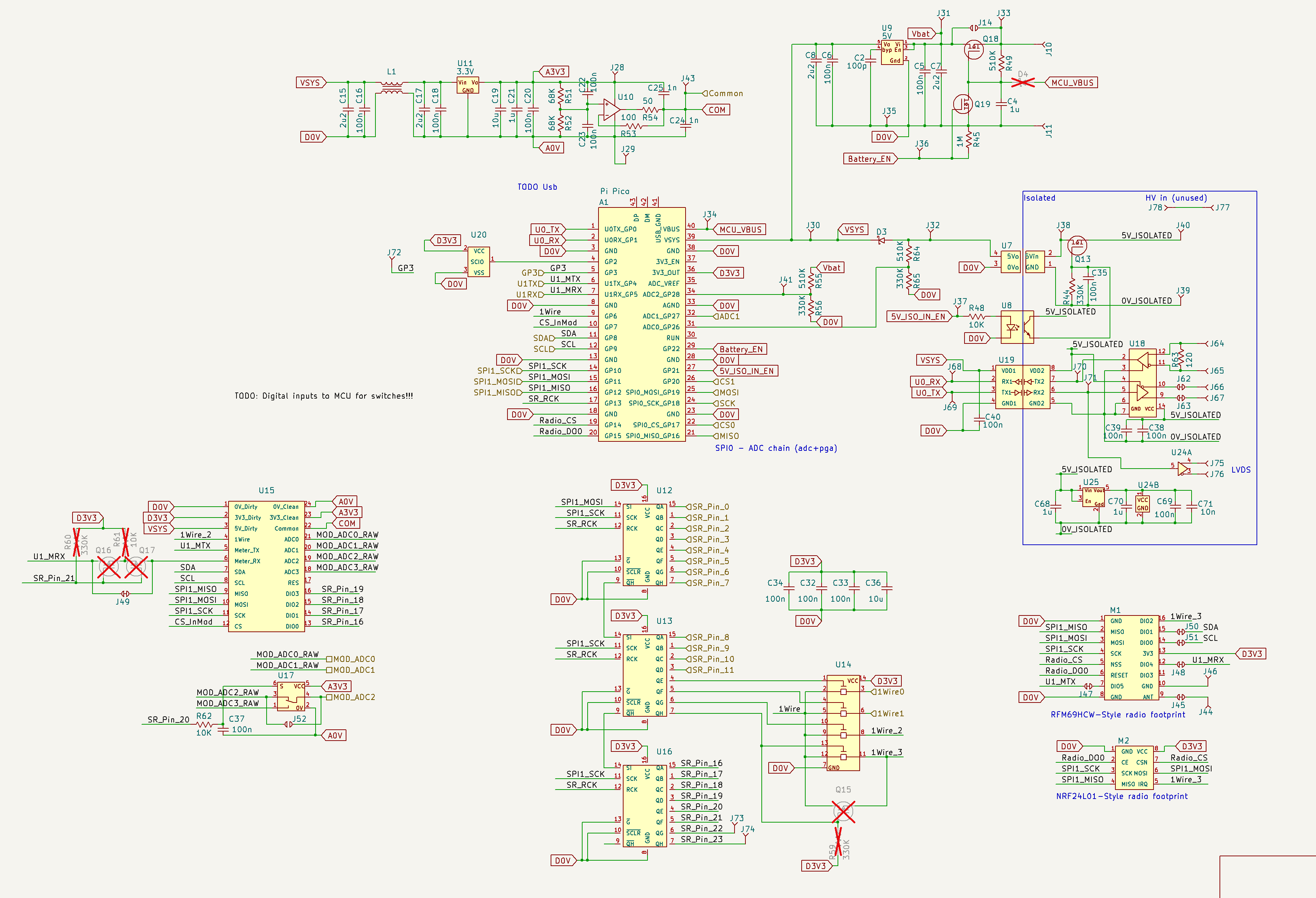
Top left we find the amp that generates COM from earlier, over to the right of that is the battery input. There's a pfet to allow it to be disabled if we're running on external power or if we want to soft-power off. When powered on, C4 is discharged and will hold Q18's gate low at first, keeping it on. It takes about a half-second to charge, and in that time, the MCU has to turn on and pull Battery_EN high, which will keep it on permanently, or this pfet will shut off, and we'll lose power again. For an auto-power-off that will actually cut all power, we just drop Battery_EN to ground, and it will allow Q18 to shut off, completely cutting off the battery power.
From there a simple 5V linear reg feeds that to VSYS, which notably can take 5V at its output without drawing significant current or backing that through to the input. Is also very low drop out and will pass voltages below 5V to the output, so we *can* run with a battery voltage, and thus VSYS, below 5V. The Pi Pico handles this just fine, and pretty much everything else runs on 3V3 (the only regular part running directly on VSYS, the digital isolator, U19, can tolerate down to 3.3V as well).
M1 right in the middle is a pi pico, not really much to say there. Notably it should be able to be replaced with anything else with a pico form factor, may come in handy if we want to use something else at some point.
Section on the right is the isolated communication part. I wanted this to be able to talk to, and be powered by, anything without having to worry about isolation in that part. U7 passes isolated 5V DC, U8 is just a control signal to turn that off, though I probably won't end up populating this and rely on the other end to disable its output, I wanted the option. U19 is a digital signal isolator, used to pass a full-duplex UART. U18 is a TTL to RS-422 converter, the main way this talks to the outside world is RS-422, so we can use long cables if desired. This whole section will go to a DB9 connector. If we want to say, log to a computer far away, a simple USB-422 bridge will allow a pretty basic cable up to reach 10's or 100's of feet. The last part, U24 and U25 is an option for an LVDS transmitter, this will allow for higher data rates, U19 can handle up to 100Mbit and this can go up to 400. Not quite as robust as RS-422 but might be interesting to have, especially for doing something like high-rate streaming. Don't think the pico's UART can even hit 10Mbit by default but may be a way with PIO or something. U25 is just a 3V3 regulator for it.
In normal operation, the screen will attach to the rest of the meter through this DB9. It's got a separate microcontroller and everything and just talks to this one over UART. Again part of the modularity - if you want a different screen (like a color LCD or OLED or something, or some processing grunt, or whatever, you don't have to redesign/remake the whole thing, just an MCU, screen, battery, and RS-422 transceiver. Plus then we can have a remote display from the whole front end, either with a cable or even wireless:
M1 and M2 are radio modules, footprints for both the common RFM69HCW and NRF24L01 modules. I've used both a ton, love the RFM69HCW for the range and reliability, it's a fairly low-bitrate 915Mhz radio. Back in 2016 I retrofitted an old VHF R/C radio with one of these, and made some receivers with attiny84's, for my quadcopters and planes, been using them ever since. The NRF24L01 is great because it's cheap as chips and you can get them everywhere. Not as good range but can be much faster. I wanted to have some option for wireless coms that ISN'T bluetooth to a phone. It's a short range, unreliable, annoying to set up protocol AND requires me to use my phone to use my multimeter? No thank you. Planning to have a radio in both the front ends here and the screen, so the whole screen module can be detached but still operate normally. For the RFM I've also got a couple other things connected to some GPIO that that chip has, I don't plan to use them with that radio, but should allow for a serial or I2C controlled module in the future instead.
U12, U13, and U16 are some regular ol' shift registers, just didn't have enough IO on the pico to run everything. I realized in writing this I need a couple inputs as well (to read the switches to control everything and enable ohms and mA range), so I still need to add an input register. Oops. Not really much going on with these in any case.
U14 is used as a digital mux, to connect a pin from the MCU to any module to talk 1-wire to it for ID purposes. Q15 and R59 are potentially a replacement for that, to cut down cost. Since 1-wire is pulled up by default, the devices are on the source side, and devices never initiate a transaction, it *should* work with just 1 p-fet, If it were backward the body diode would conduct and ruin everything, but this should be fine. Not fully implementing it in this version (which is why Q15 and R59 are DNP), to save space, but do want to be able to test it. U20 is a 1-wire EEPROM that's on this board, to store some basic hardware info about the board, maybe even calibration info. That way, again, the MCU firmware can be common to more than one design, without having to change if different boards have different parts populated, etc.
Finally U15 is the "input module" (I'll come up with a better name at some point) - the idea is that I can have some headers here with several connections available, and make smaller boards for special functions. Also, again back to that idea of modularity at many levels. Two big things I've wanted in a meter forever is a little built-in electronic load, unfused high current measurement (for things like motors and motor controllers, that have inrush current and loads in the 30-50A range), and XT-60's as input connectors.
At it's most basic, an electronic load can be *so simple*, just a transistor, opamp, and shunt resistor! Won't be able to dissipate much power in this form factor, but could do loads of a couple hundred mW or big pulses really easily. For both the XT-60's and high current range, you can get parts like this: https://www.digikey.com/en/products/detail/allegro-microsystems/ACS711KEXLT-31AB-T/3868195
which are fully isolated, do +- 30A (there's similar parts that do 50 or 100A too!), have almost no burden voltage, and can take peak currents well outside that range. Does everything I want for $1.50. Originally I was planning to build in a part of XT-60's with one of these between them to measure current and a differential input to measure voltage - wouldn't be fully isolated but good enough for little battery powered stuff, but at some point realized there's so few parts in this bit, and so many other little things like this (like an E-load) that might be *super* useful, it'd be cool to be able to swap out just this one part of the meter. So, I'm making this a little ~1"x1"x1" cube with some headers at the bottom that goes to the top surface of the meter, so I can add pretty much anything without having to redo the whole processor, power, adc, communication, isolation, case, and everything, it can be as simple as a little 3D box and a chunk of perf board and some passives. The analog switch below is because I wanted 4 analog inputs, but only had 3 left on the main mux. The DNP fets are to test muxing the UART. I've only got 1 UART left, but want the option of talking to a couple different modules (sorta like the 1-wire thing). Planning to have the standard be to have the module hi-z its TX pin until the mcu asks for something, but might be nice to have the option to have the mcu control it instead. Probably won't use this for anything until the next version, just want to test it for now.
Aaaaaand I think that's everything!
This ended up being way longer of an explanation than I expected, but served as a good rubber ducky of the design, found a couple little things I needed to change/fix during it.
And we're on to layout!
Discussions
Become a Hackaday.io Member
Create an account to leave a comment. Already have an account? Log In.