 michaelk99
Layout Considerations
- 4-layer PCB stackup: signal/ref(0V)/ref(0V)/signal
- place analog and digital parts as far as possible apart from each other, to reduce cap./induc. coupling
- local decoupling at each power pin of each IC + vias to reference planes near the power lines
provide a defined return path! - use dedicated ground traces from charge pump inverter pins to decouping caps --> reduce coupling into plane
- no reference plane under crystal
Schematic/Layout Concerns - Low Noise (rework in progress)
Rev1:
For now I have chosen the LT1028 as op-amp, as this part was suggested by the DAC's datasheet (PCM1794A) due to is ultra low noise performance.
LT1028: input noise voltage density at 1kHz of 1.2 nV/rtHz max, but this comes at the price of ~10€/part. So this raises the question, if any switching noise of the digital part etc. would be much higher than this.
Alternative part used by "Project-1": OPA2134 (8nV/rtHz @ 1kHz), its half the price
Rev2:
- Complete Power Supply Redesign:
Replace 3.3V charge pump with LDO (digital supply for DAC)
lower op-amp supply to +-4V to ensure proper operation even when USB voltage is only 4.5V --> use LDOs on both rails for enhanced isolation
- Amp. Circuit Redesign:
- Replace 22Ohm resistors with proper I/V op-amp stage (gain+filter) (OPA1612)
- Diff2SE Stage, no gain (OPA1622, higher output current)
- Global Feedback from Diff2SE back to I/V
- --> Stability issues, simulate loop gain,
- Amp. Circuit Redesign Rev2.1:
- Do not use a global feedback loop as the current circuit does not seem to work probably.
- Go with datasheet circuit from OPA1611 opamp for a decent first design
this circuit uses the same I/V stage and a diff. multiple feedback analog filter as second stage - TODO: optimize gain setting resistor and validate performance for main target headphones
Stability Issues with Rev2 Amp. Circuit (work in progess)
On hold for now due to a lack of time. Although, the Rev2 amp may not work as intended.
- LTSpice Sim. (see gallery)
- Transient: Oscillations of ~ 700kHz, sim did not finish
- Loop Gain sim: break up loop for AC(consider Rosenstark's loop gain measurements)
https://www.edn.com/middlebrooks-and-rosenstarks-loop-gain-measurements/
- Break up loop at input of I/V stage as input is a high imp. node (Z1) compared to output of diff. stage amp + feedback RC (Z2) --> Z1 >> Z2
- If current sim gives valid results (validate!), the open loop gain T(s) does not satisfy certain conditions to apply the nyquist criteria ( |T(s)| < 0dB, s--> Inf). Modify T(s) that nyquist may apply --> modify T(s) to create a stable loop
USB Inrush current limitation
USB 2.0 limits the VBUS capacitance to 10uF
- soft startup with mosfet?
- dedicated IC?
- NTC?
Layout Concerns - USB (resolved)
Plan on getting the first PCBs manufactured by OSH Park, but need to validate the layout first.
Since a USB-C connector is a must for this project (future-proof connector), I may get some issues with how I connected the two instances of D+/D-.
Did some TL impedance calculations for the USB lines based on the micro strip approx. given by Pozar (Microwave Engineering) for a single ended (45 ohm) line, see the matlab script. Checked the line width for a differential pair (90 ohm) with this calculator: https://www.eeweb.com/tools/edge-coupled-microstrip-impedance/
So the traces on the current layout should meet the 90 diff. impedance requirement. However, the traces are thinner at the beginning, as the connector has a lower pitch.
I assumed a rise time (USB) of 8 ns, did some measurements with a USB 2.0 FTDI Serial bridge and my DS1054Z (hacked). So I'm not sure if this scope is suitable for this kind of measurements. With this assumption, the line lengths (propagation delay) should be low enough to assume lumped elements (tcrit = trise/4, tdelay < tcrit), see matlab script as well.
Further, I assumed the thinner traces (10mil) at the connector, as some additional TLs (matlab script) and calculated a potential...
Read more »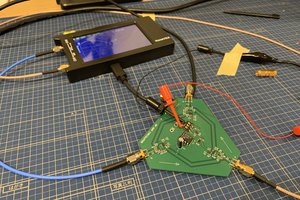
 nijichichi
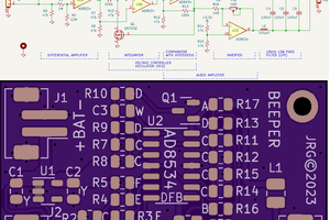
 Ghani Lawal
 Nick Sayer