 Tim
TimDesign Goals
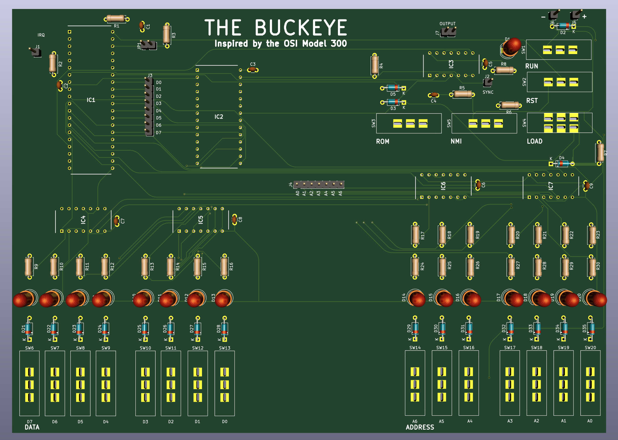
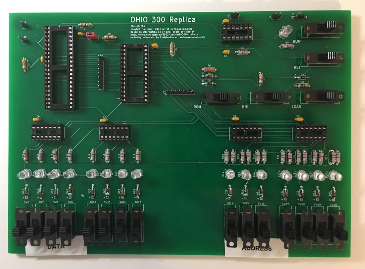
- Restrict address space to 128 bytes of RAM by having only seven switches like the original even though unlikely to find physical RAM smaller than 64K
- Use modern, easy to source components
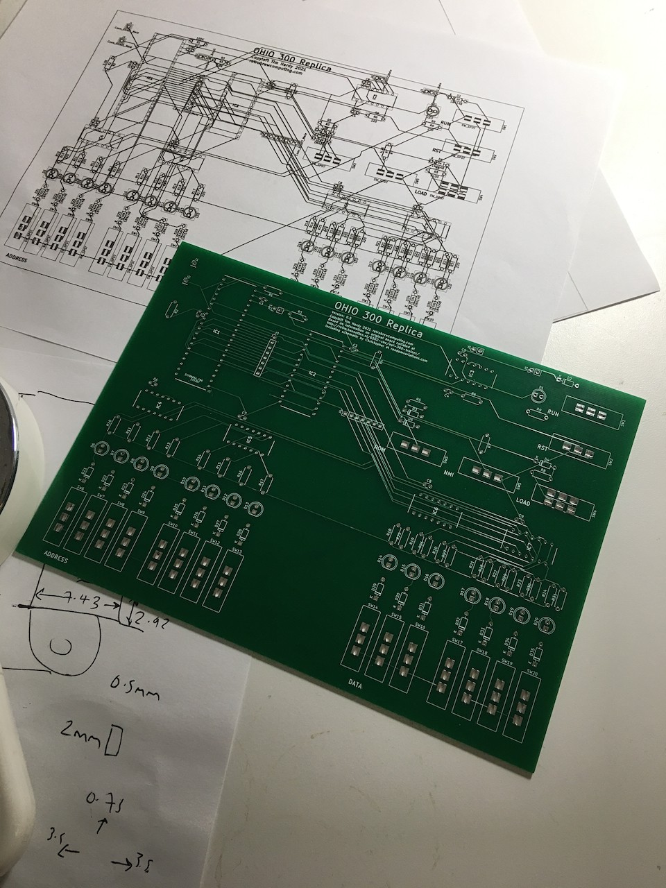
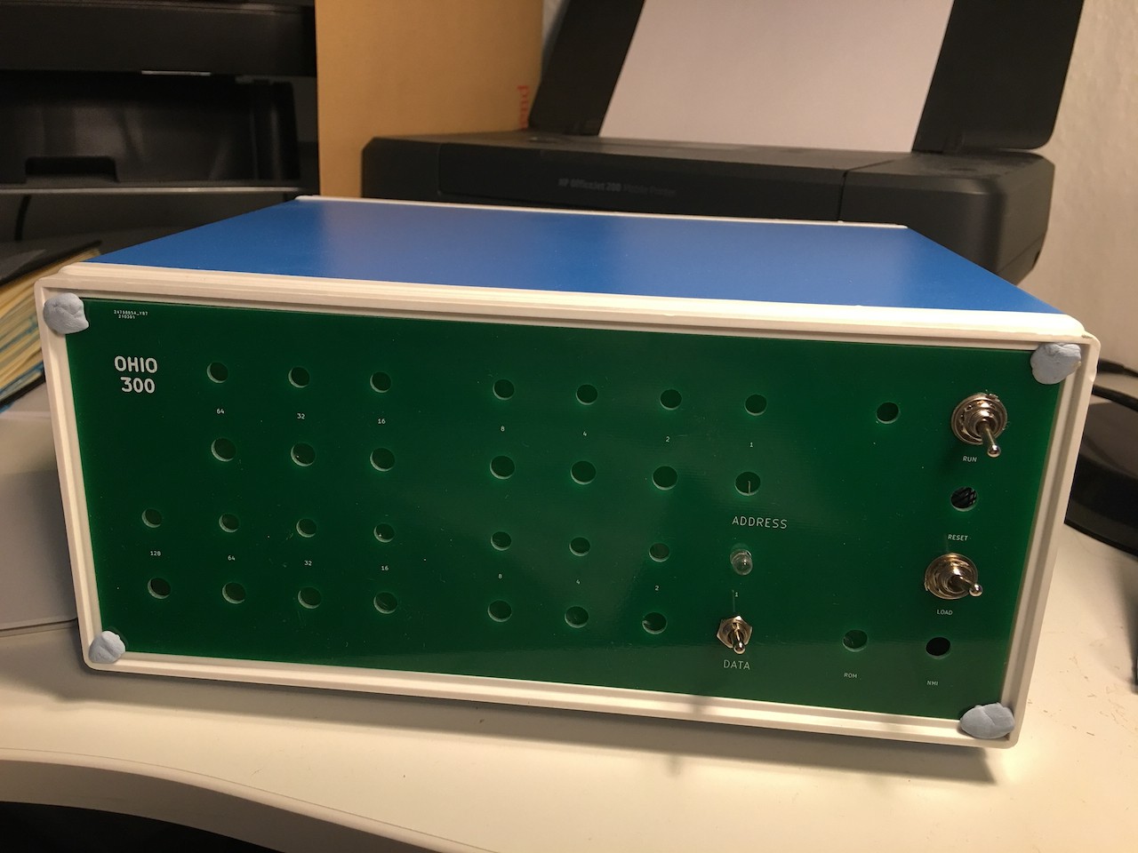
- Make board large enough to use comfortably, small enough to ship cheaply
Stretch Project Goals
- Include expansion points that might make it easier to add a ROM and address more RAM
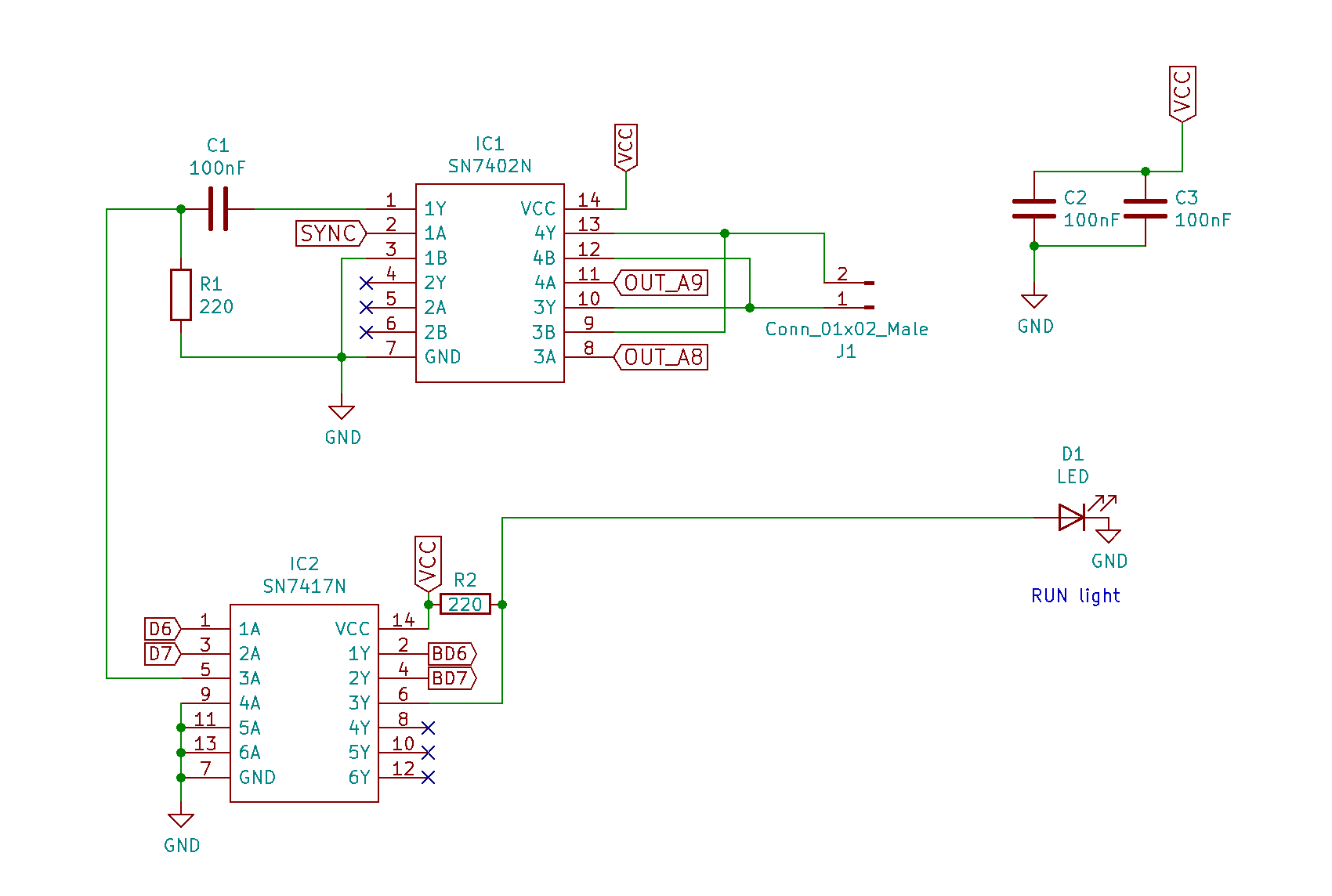
- Replicate aesthetic of hand drawn traces
Financial Goals
- Sell a few bare PCBs to cover costs of prototypes
- If sufficient interest, try selling a small number of kits
Personal Learning Goals
- Learn basics of electronics
- Learn how to read and draw a schematic
- Learn basics of Kicad
- Work through original OSI 300 manual with completed board and grok how it works


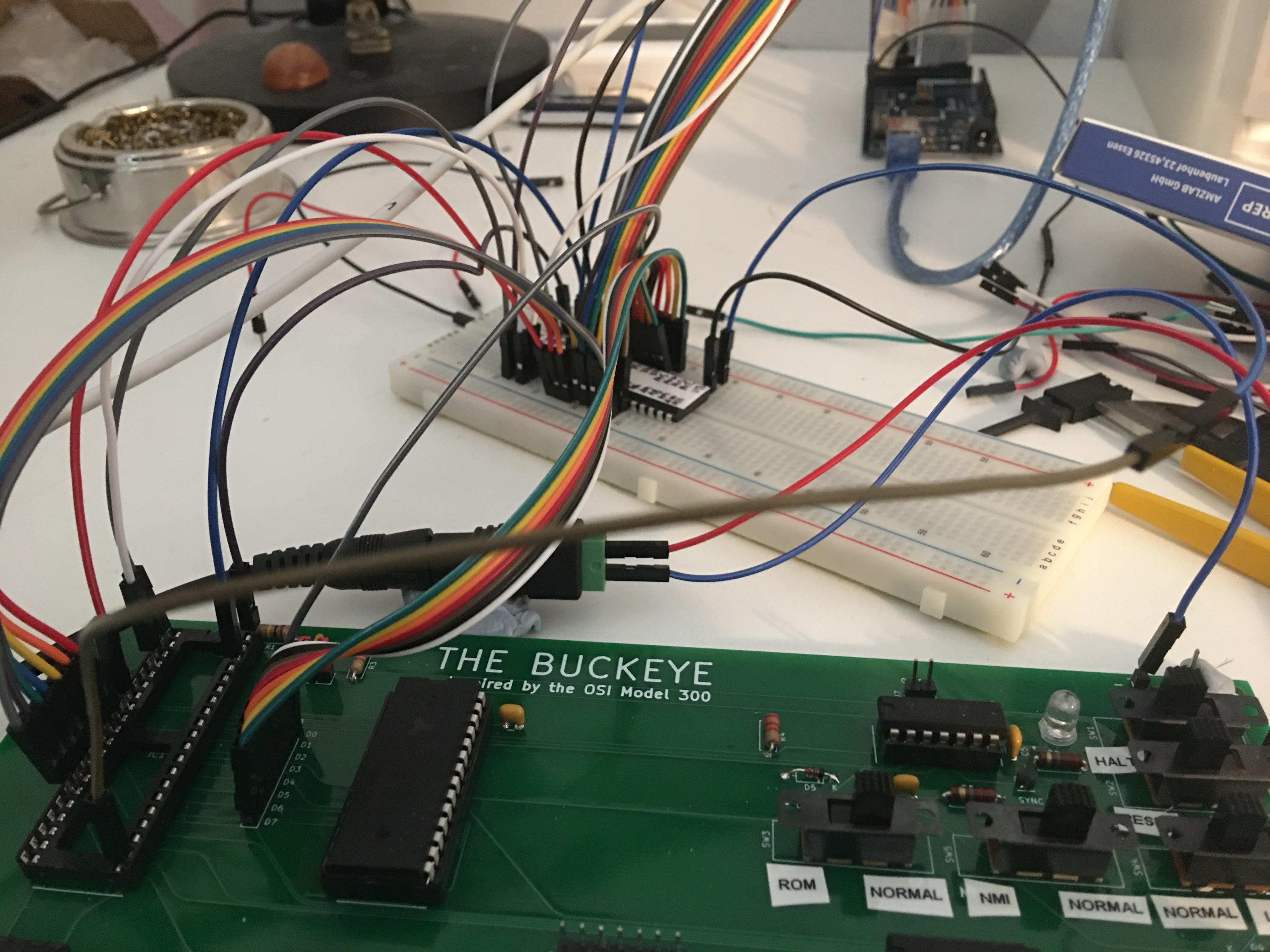
 With time off over the bank holiday weekend, I've made some progress.
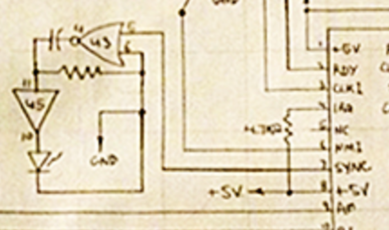


 blinkingthing
 Gee Bartlett
 Jackson Keating
Hi Tim, I found your project while searching for information about the OSI 300. I wanted to try and recreate it as well, but I my knowledge of electronics is self taught. Is your project still ongoing?