Close
0%
0%

Basic MC6800

Building a simple striped down computer from the mid 70's based around the Motorola MC6809 MPU

Similar projects worth following
While I was diving deep into Verilog and FPGAs I came to the conclusion that my knowledge of system design is very limited. So this is a project to help me to further understand computer systems. The idea is to try am making the most basic system possible with a few limited resources mainly containing just a RAM and ROM and access to the systems data and address buses to experiment with adding peripherals further down the line.

For this system i decided to select the Motorola MC6809 MPU

There where a few reasons for this selection I wanted to use a processor from the MC6800 series they where 

  • Prolific as the processor of choice in many arcade cabinets. 
  • The layout was easy to understand.
  • |t doesn't require much in the way of supporting hardware. 
  • I felt it was a bit of an unsung hero as most people focus on the MOS6502 and the Z80 CPUs

The project for me is getting a CPU running and taking to other hardware using system buses and control lines and how this would interpret into FPGA fabric.

The MC6809 specifically has the ability to run directly for a xtal crystal which made it much simpler the the MC6800 which requires two clock pulses at specific intervals  
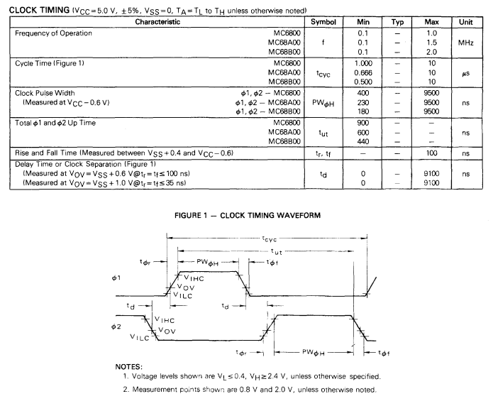
This is the complicated clock requirements of the MC6800 the is an ic made by Motorola the MC6875 clock generator, but these ICs are rare and expensive. 

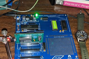
The board is going to be simple just enough to execute code so RAM, ROM and some simple glue logic. 

  • 1 × MC6809P Microprocessors, Microcontrollers, DSPs / Microprocessors (MPUs)

  • New PCBs have arrived

    Gee Bartlett08/20/2020 at 21:44 0 comments

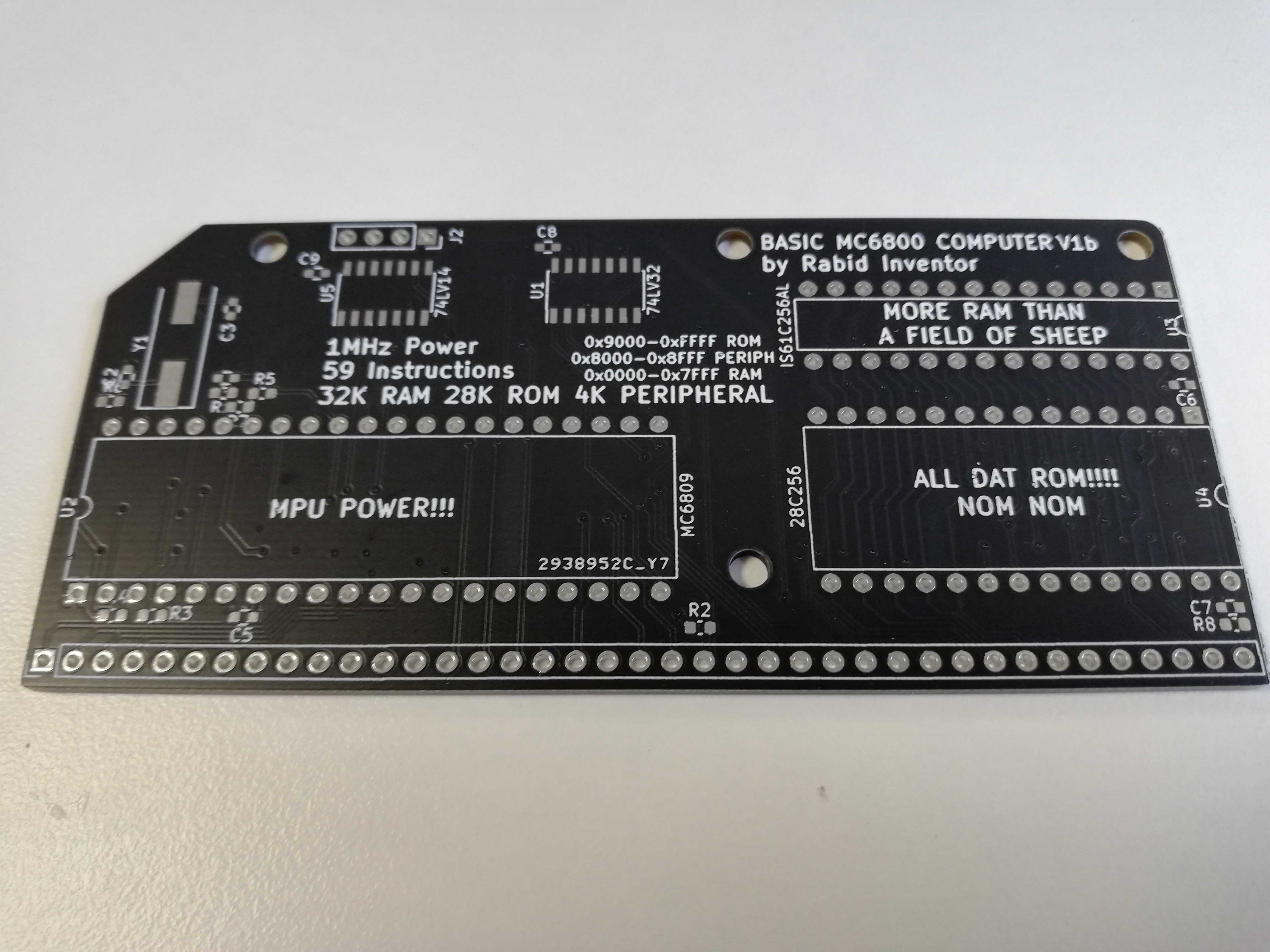
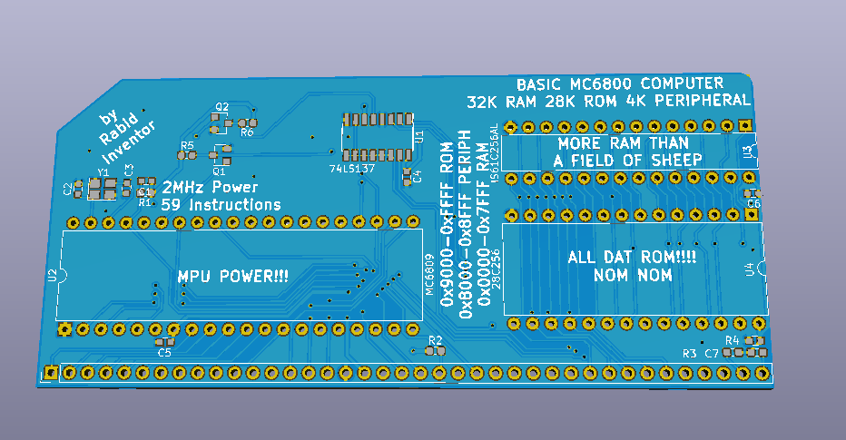
    Super excited to get a little box from JLCPCB. To find the next version of The Basic-MC6800 V1b. 

    Really loving how the boards are starting to look. Black was really the way to go. 

    The finish is nice and clear as well. Really looking forward to getting the other parts for this and building them up.

    Over the last few months I have been putting some time into researching the MC6809. The processor is quite well known and is used in most of the Tandy TRS-80 colour computer range (The COCO). which Incidentally has led me to spend lots of time listening to the COCO Talk Podcast. I have also found out that the Hitachi 6309 would also be a good fit for this board with faster clock rates and low power overheads. could be something to experiment with later.

    So at the moment I'm just waiting to get some parts to build 1 or 2 of these and see if i can execute some code :)

  • Basic-MC6800 where am I now

    Gee Bartlett08/02/2020 at 06:40 1 comment

    Thought it may be time for a brief update as I have been quiet on this for a while.

    The Basic-MC6800 is still an active project it has just been n the back burner for a little while while i have been working on other things.

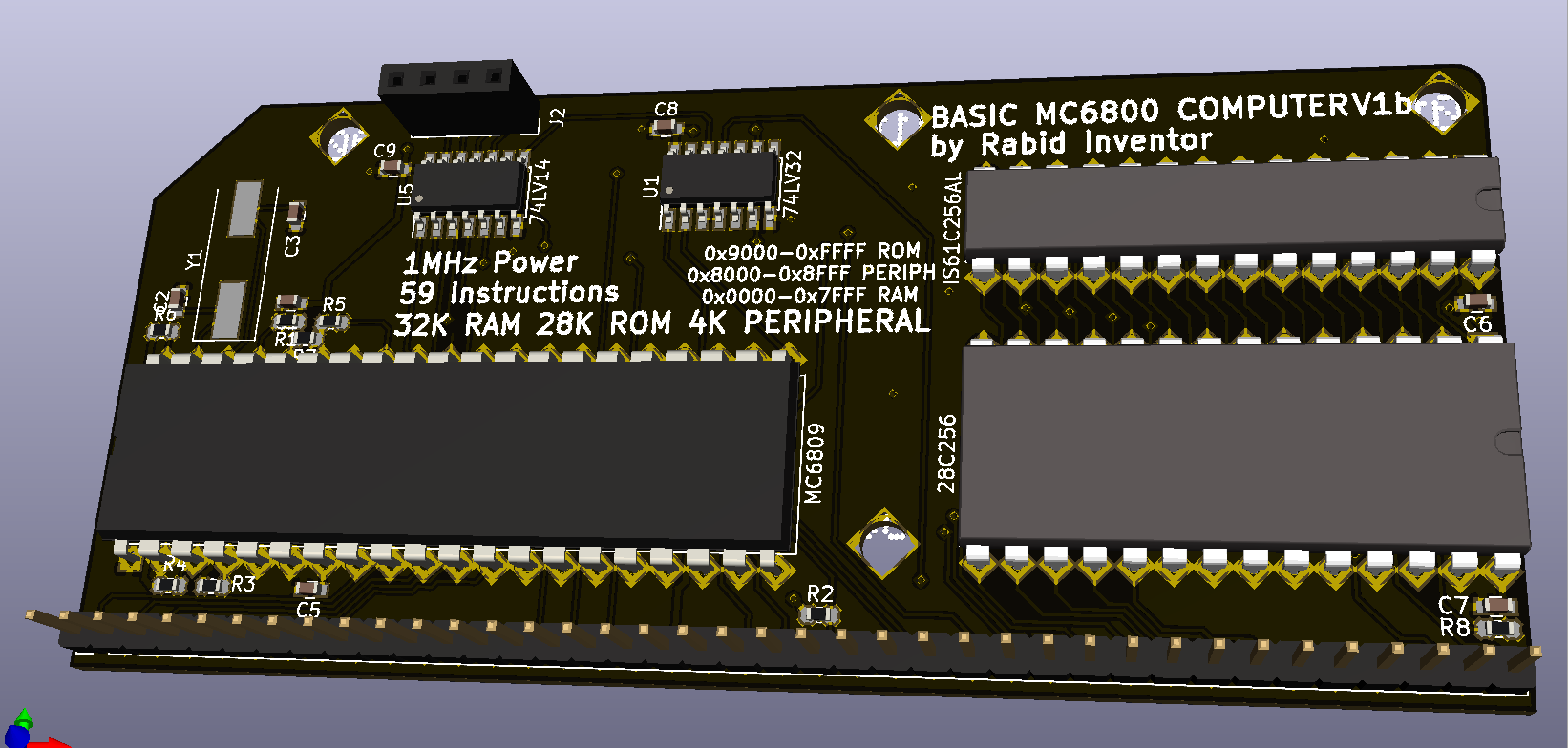
    I have pretty much completed the next version of the board. It is now waiting to be sent off the JLCPCB. 

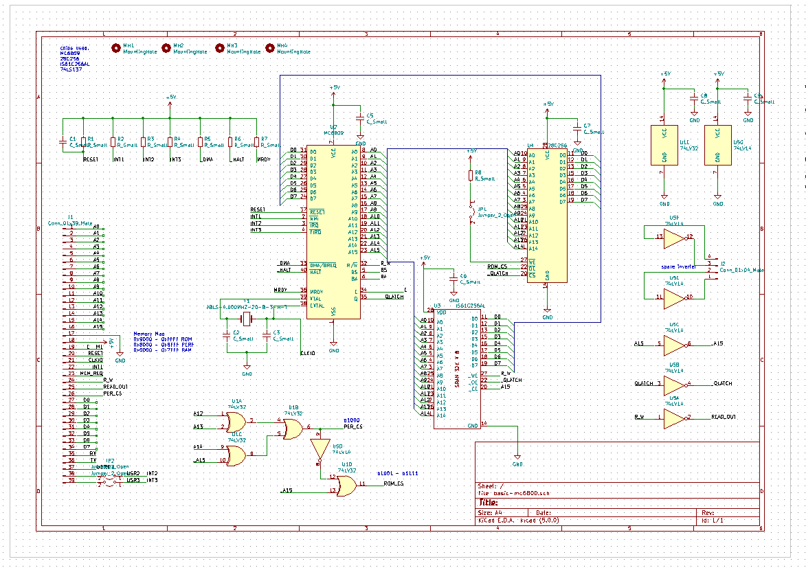
    I have made some updates to the control logic using a set of and and or gates so now the control logic should work.  I have also broken out a few spare inverters just in in case they are needed for modding later.
    I have added a series of mounting holes so I can add future boards on the front. The other thing to not is i Changed the crystal package over the a HC49 landing as these are more freely available in for crystals < 4MHz. 

    Looks the part in the 3d render.

    Still wondering if the skinny DIP is the right choice for the RAM.

    This project slowed after the Retro computer fair i was going to take it to was closed down but ii'm getting a feeling for continuing this project further. 

    I'll keep you updated how things go.

  • Testing Testing

    Gee Bartlett05/06/2020 at 07:32 0 comments

    I managed to build one of the REV1 boards and have been spending some time on an off working out all the kinks before going to the next version.

    i decided not to puth the decade counter on for the moment though that will be something i will come back too. 

    I also found some issues when it came down to the pulling of certain pins.

    Out of habit i had already added pull-up resistors to the interrupt pins to try and keep them stable aslos the same situation with the reset pin. 

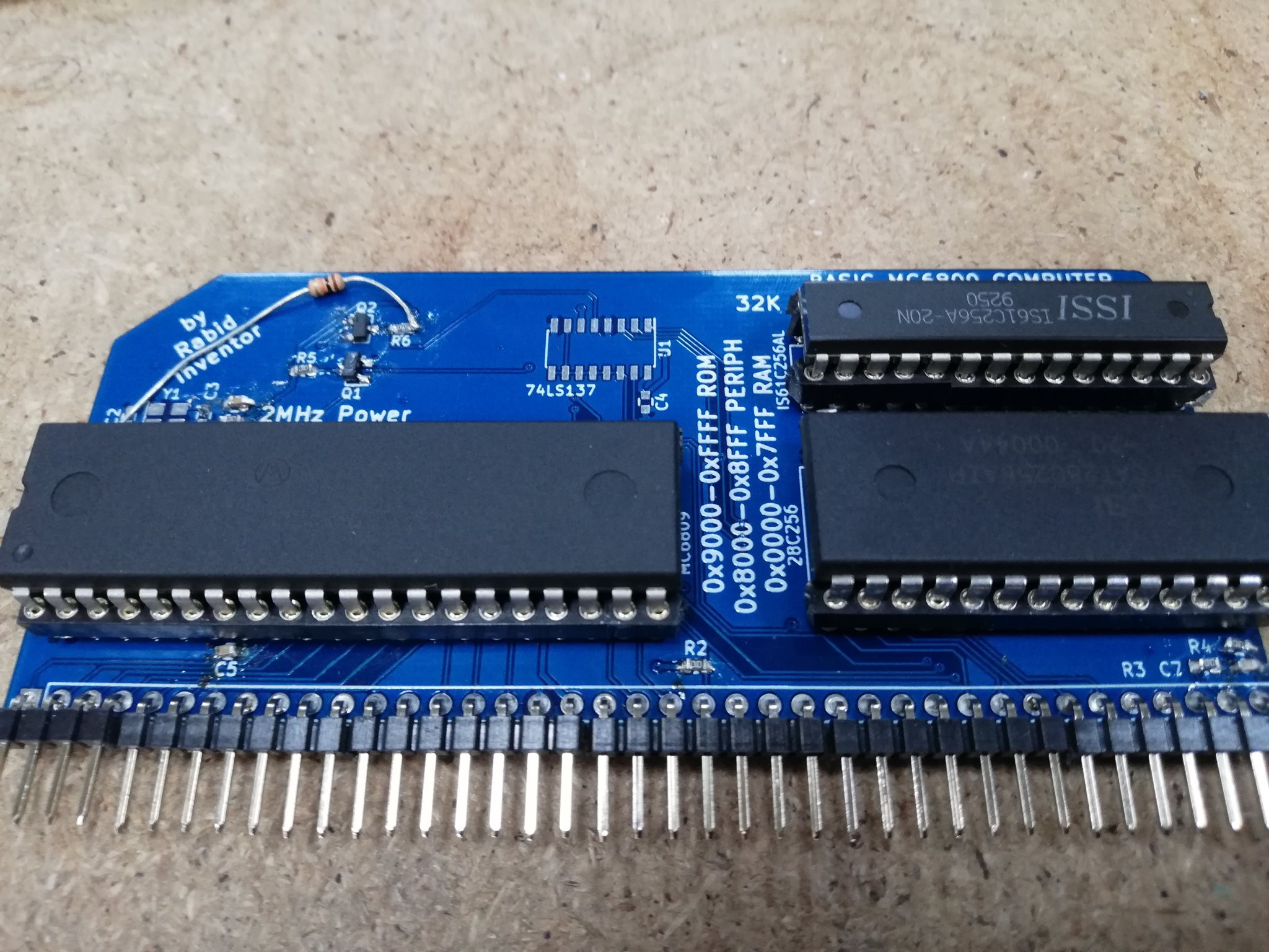
    Soon after I  found out that the reset pin has no internal pull-up resistor either so that is the reason for the resistor that can be seen in the above image.

    The other issue was the when the device was free running it would swap between different speeds. A0 was jumping between pulsing at 100KHz and 10kHz and when i touched the back of the board in a certain way it would stabilize. 

    After a little further investigation I discovered the DMA request pin didn't like being left floating as it would issue a dma request which cause the Processor to release the address and data bus for up to 16 cycles.

    The final fault that i am still trying to thrash out before moving forward is running from a xtal so far the only way i have had the chip running is a buy using an arduino to generate the clock signal. 

    As you can see in the above video the processor is free-running and showing the output form A15 and A13. which give a 1:4 flash pattern. It easy to also see where the clock signal is patched in.

    Last thing to check is can it execute instructions from ROM and can it store values in RAM once these are tested I can move forward with REV2

  • Rev 1 Arrival and some chips

    Gee Bartlett03/29/2020 at 11:37 3 comments

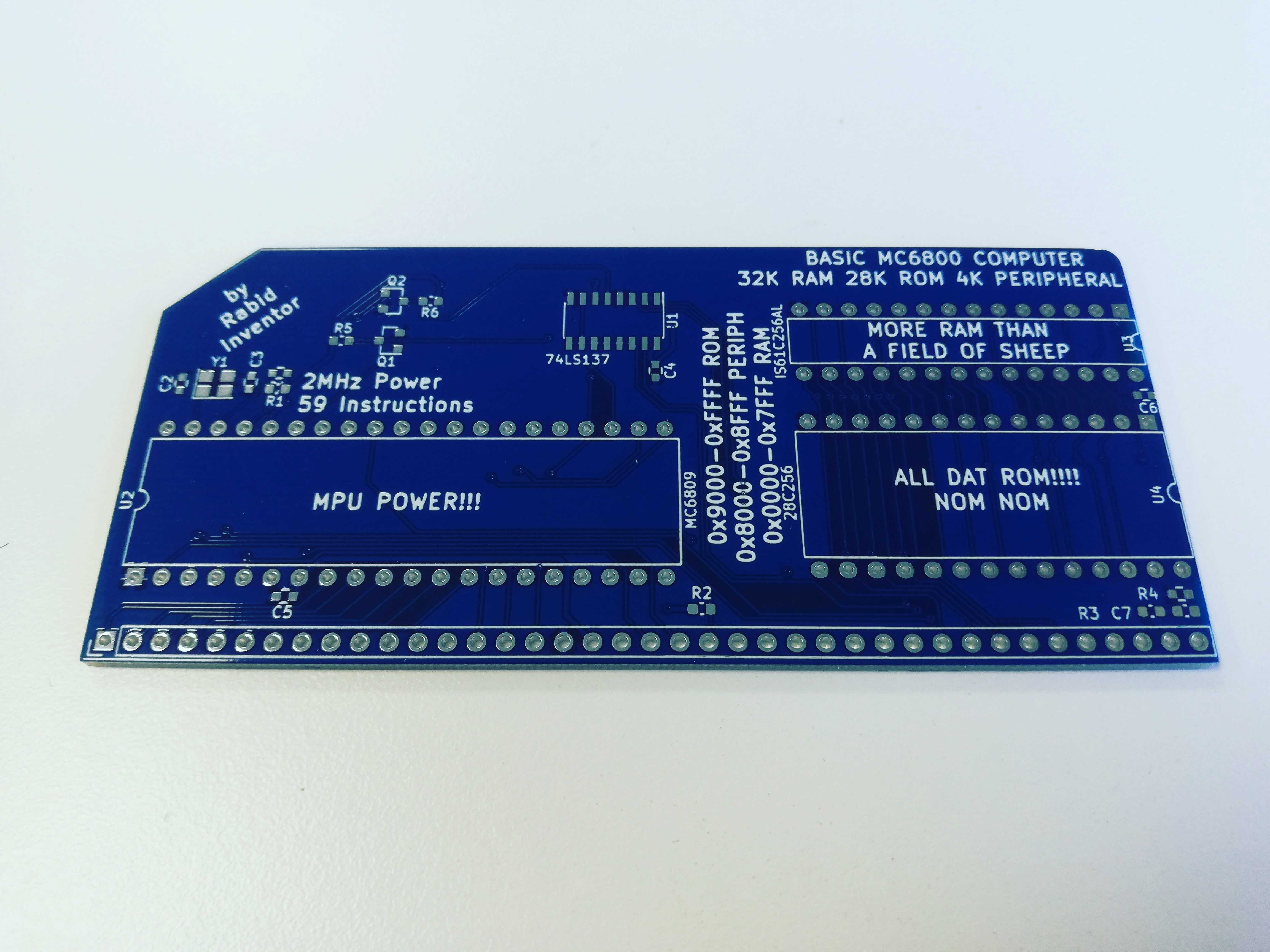
    I always feels nice to receive a PCB you have designed.

    Even though I know that there is a problem with the ROM and peripheral selector on this board i feels good in the had and should give me enough to work with at least to see it running. 

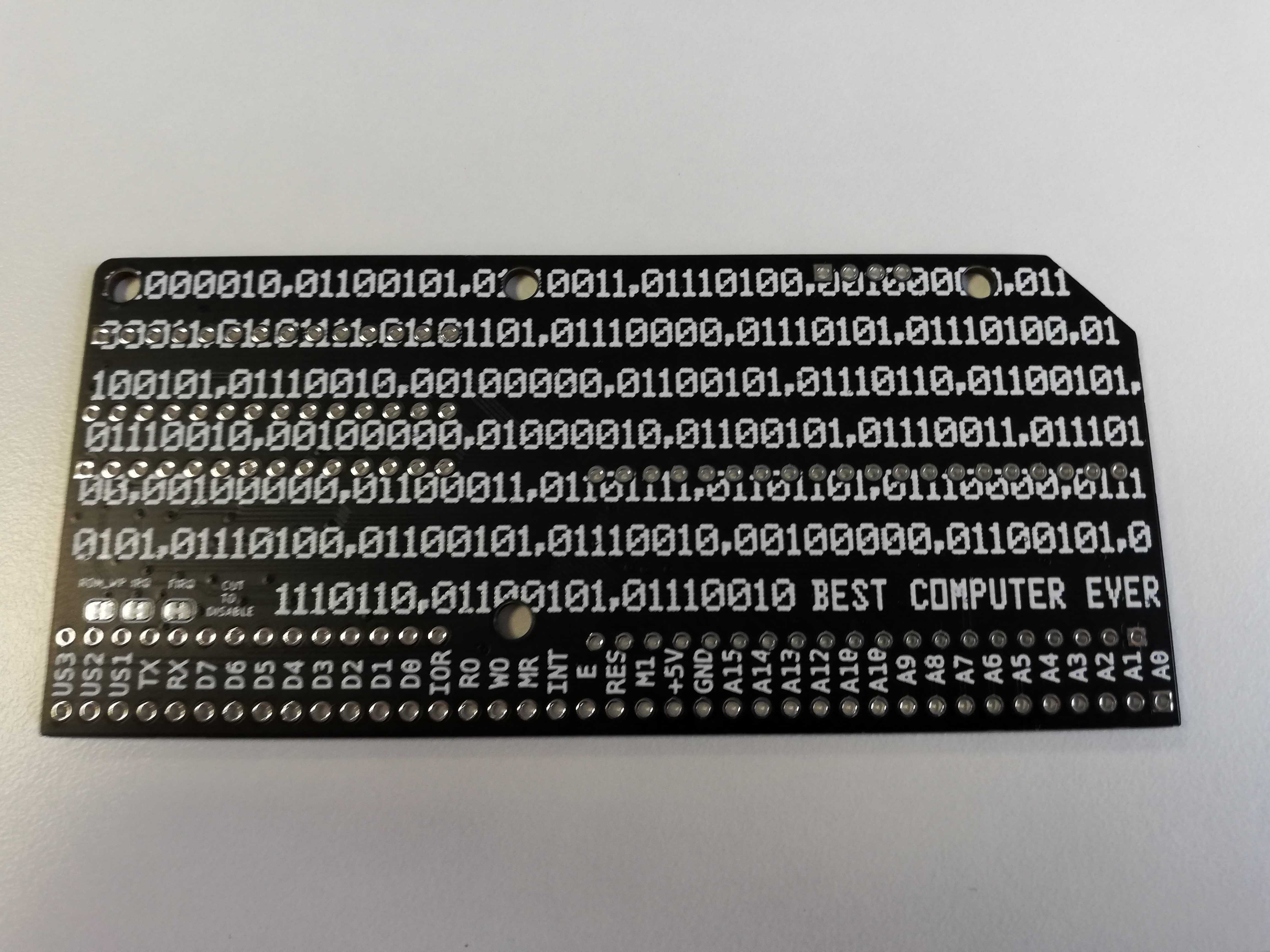
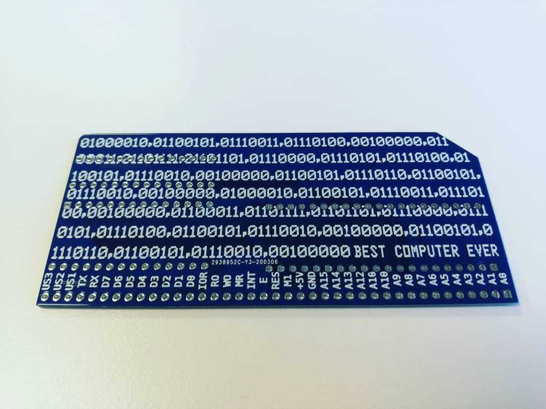
    Really pleased with how the silk looks, by the way the bin is ASCII (nerdy i know) :)

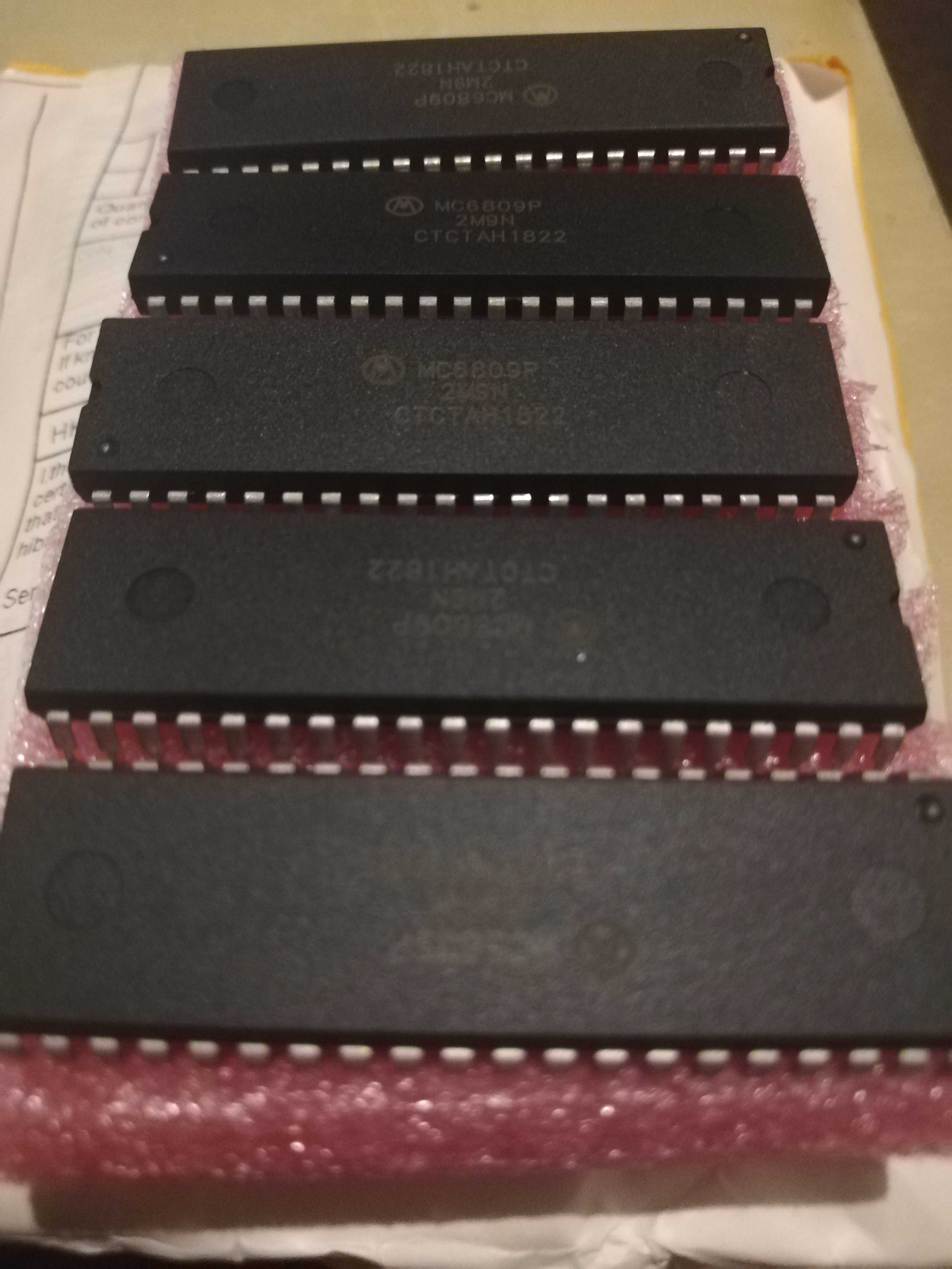
    another nice arrival was the Processors themselves surprised about the date code week 22 2018 so reasonably new chips  looking in great and unused condition. I am hopeful for these i need something to set the free running though.

  • sorting the logic

    Gee Bartlett03/13/2020 at 09:28 0 comments

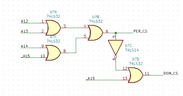
    After my mistake with bridging the outputs of a 3 to 8 decoder I have been taking another look at the address logic. I believe that I can use OR and NOT gates to do the selection between the ROM RAM and peripherals. I have come up with this. I still have to check it with a logicsim but seems it sane. the nice thing is I can use some of the spare NOT gates for the Q and A15 inverters so extra bonus.

  • OOPS but I think I have it now

    Gee Bartlett03/07/2020 at 18:52 0 comments

    So.......

    As pointed out here and on twitter I have my decode logic for the ROM and Peripheral addressing a but wrong. 

    well blue magic smoke kind of wrong :D

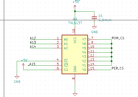
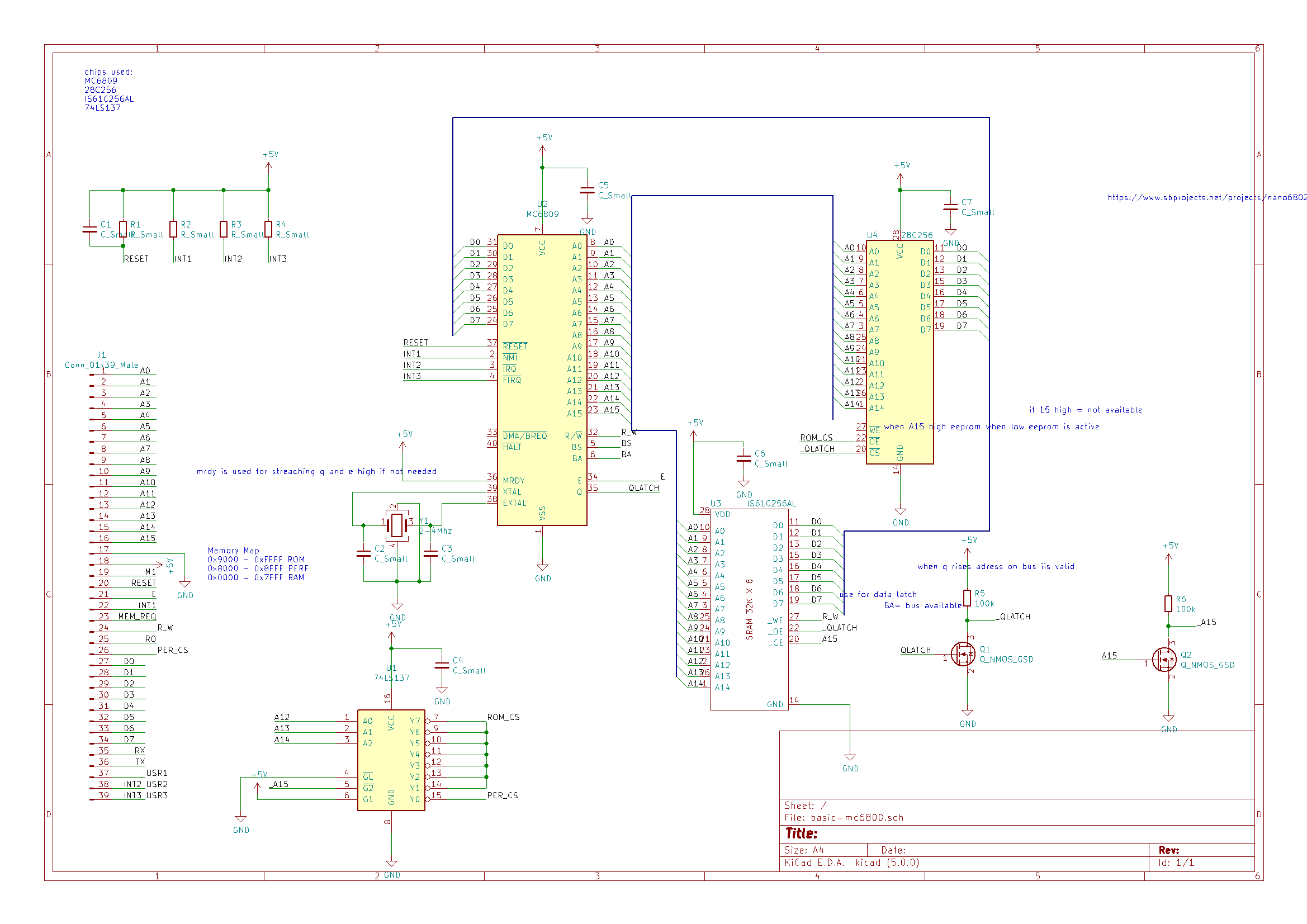
    this circuit

    would mean that if any of Y7 to Y1 are active then it would sink the the current from the rest. The high state of each gate is provided by a 120ohm resistor this means, 6 x 40mA would sink into the active gate.

    There is not really a way to bodge this well so on this pin of the board i am going to hardware _A15 to ROM _CS or maybe do something else of board.

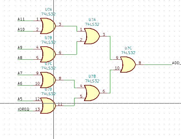
    I'm experimenting with ideas but i think my final solution will look something like this.

    using multiple OR gates to drive the select line. I this format I think the select will be low only if every input is off. this is taken from the IO board I am currently working on.

    Let me know what you think......

  • First PCB spin designed

    Gee Bartlett03/05/2020 at 21:24 0 comments

    Finished the initial design the 64K address space is divided up as so. 

    0x0000-0x7FFF RAM 

    0x8000-0x8FFF Peripheral space

    0x9000-0xFFFF ROM 

    I initially had the ROM at the bottom of the address space and the RAM at the to how every thanks to many people on twitter I was informed that the Reset Vector this is a memory address that contains the first address to execute code from should be contained in ROM (this is something I didn't know before this project). The Reset Vector for this MPU is 0xFFFE right at the top of the address space so the RAM and ROM got swapped.

    I decided to use a 3 to 8 decoded to select the peripheral instead of basic gates The reason is if i want to add a display buffer or other device i could take a lead form that sacrificing 4K of ROM space.   

    _A15 is the inverse to A15 generated by a FET and pull-up resistor so it goes low when A15 is high. I also needed it to select between this and the RAM at the bottom of the address space. 

    This the full schematic have been over it several times and believe cleaned up any issues. 

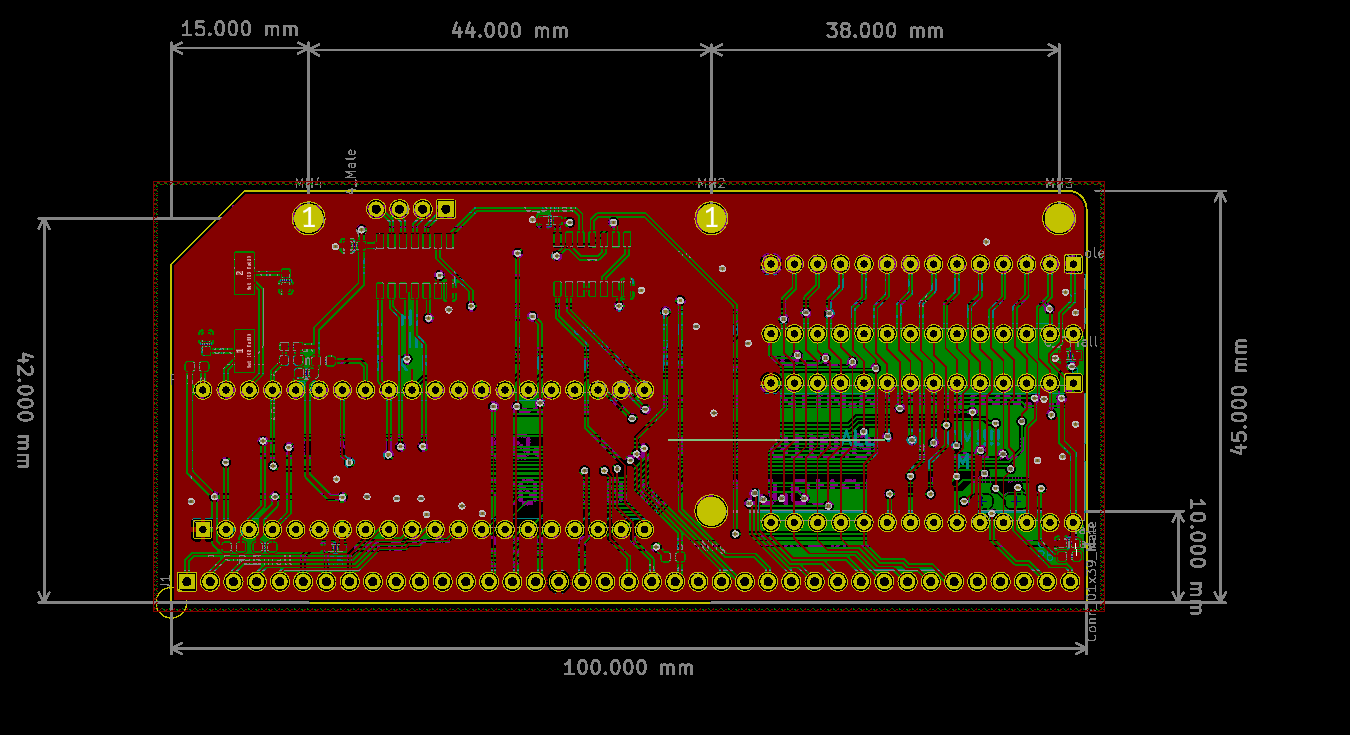
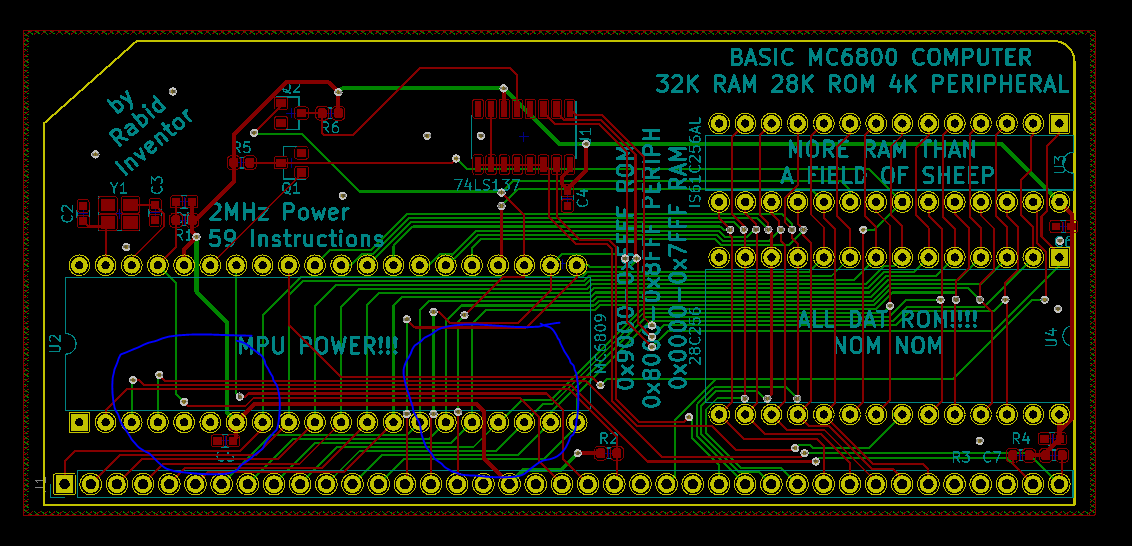
    This is board almost as it has been sent off to the board house I did some more trace optimizing and managed to remove a load of vias.

    As you see in the area I have marked in blue.

    So now the PCBs are ordered with JLCPCB so just a waiting game.

    wish me luck :)  

View all 7 project logs

Enjoy this project?

Share

Discussions

Gee Bartlett wrote 03/06/2020 at 08:42 point

I asked myself the same question after I sent it off my first layout was going to use add gates for the peripheral select line which meant _A15 was used directly to the RAM select (when i had the memory map upside down). The LS137 wiring means i can cut between traces and patch of extra selects if i want them. 

I have BSS138's laying about and freely available so just making FET inverters just seemed natural. i'll have another look at the enable logic.

This is really a live and learn project I highly suspect i will have plenty of bodging to do on this version. :) 

  Are you sure? yes | no

Steve Toner wrote 03/06/2020 at 17:43 point

Here's the problem with connecting the Y outputs of the LS137 in parallel:
The outputs are what are called "totem pole" outputs.  There are two transistors, one of which is on at any given time.  If the output level is high, a transistor connects the output to +5V through a (nominally) 120 ohm resistance.  If the output is low, the other transistor connects the output directly to ground.  For the purposes of this discussion, let's assume the transistors are perfect switches - they have no resistance from collector to emitter when on and infinite resistance when off.  So you have 7 outputs connected together.  When a ROM address is specified, 6 of these will be high and one will be low.  The one low output therefore has to sink 250mA of current (approx 42 mA from each of the 6 high outputs) - plus whatever current is presented by the input(s) it is driving (minimal in this case).  And it's only designed to handle like 8mA, so it probably won't last very long...

  Are you sure? yes | no

Gee Bartlett wrote 03/06/2020 at 21:50 point

Well oh darn :) looks like a new board spin is in order. This is exactly the reason why i'm going this project, to help bridge the gaps in my working knowledge. 

  Are you sure? yes | no

Steve Toner wrote 03/07/2020 at 17:58 point

I always plan on having to make multiple revisions of a board.  But I usually end up not bothering, as I find a workaround that involves cutting traces/adding little blue wires or gluing additional chips (or even small bodge boards) to the existing PCB.  Of course, if I were to want to make more than one board (e.g., sell a kit or something), I'd end up revising the PCB...

But meanwhile, you can cut Y1-Y6 and just us Y7 for the ROM.  That'll give you 4K of ROM to play with, which is enough to be useful :-)

  Are you sure? yes | no

Gee Bartlett wrote 03/07/2020 at 18:57 point

I have thought of what to do on the next spin but for now going to wire _A15 straight to _CS  i need to make sure that 0xFFFE is in the ROM space as it will contain the reset vector.  might even be able to hand wire something to save this anyhow :)

  Are you sure? yes | no

Steve Toner wrote 03/06/2020 at 06:42 point

? Why not just connect A15 (non-inverted) to G1 and save an inverter?  And btw, they do make inverter chips :-)  Why the non-standard use of a FET to provide this functionality?  The way you've drawn it up, you need 4 devices (2 R, 2 Q - 10 pins to solder) to provide two inverters.  You could do that with a single package (14 pins) with gates left over.

But then I wouldn't be wiring the outputs of the LS137 together myself...

Also, I'm not convinced the /CE, /WE, /OE logic is correct, but I've only just briefly looked at the schematic.

  Are you sure? yes | no

Similar Projects

Does this project spark your interest?

Become a member to follow this project and never miss any updates