 agp.cooper
A Toy PIMD
I would describe this PIMD as a "toy". Why? Because it is necessary to detect the target signal immediately after the coil signal has decayed below the target signal, and before the target signal has decayed below the 40 mV threshold. In the field, the ground response will mask the target signal at this point of time.
Corbyn's paper describes the ground response of iron rich lateritic soils as:
- g(t) = (1-P)*exp(-t/T1) + P*exp(-t/T2)
where:
- P = 0.08 to 0.30
- T1 = 75us
- T2 = 550us to 800us
He also presents an estimate for a target response (i.e. decay time constant):
- T = 1.8*D^2
where:
- D is the diameter (m) of the target
For a 1 cm target the estimate for T is:
- 180 us
For a 5 cm target:
- 4.5 ms
The above target decay time constants indicate that detecting targets less than 2.5 cm in diameter will be difficult in iron rich lateritic soils.
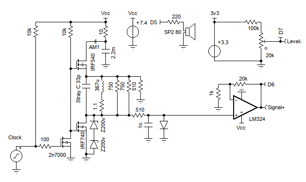
Detection Strategies
For large targets (>=5 cm), one strategy is to wait for the ground response to decay well below the target response. For example, if we have an initial 100 mV ground response and a 10 mV target response, then we could wait 4200 us when the ground response is 40 uV and the target response is still 400 uV. Assuming a 10 to 1 signal to noise ratio is desirable.
If we can filter out 90% of the ground response then we only need to wait 520 us for the same 10 to 1 signal to noise ratio.
In either case we need more gain to allow signal sampling much later in the pulse cycle.
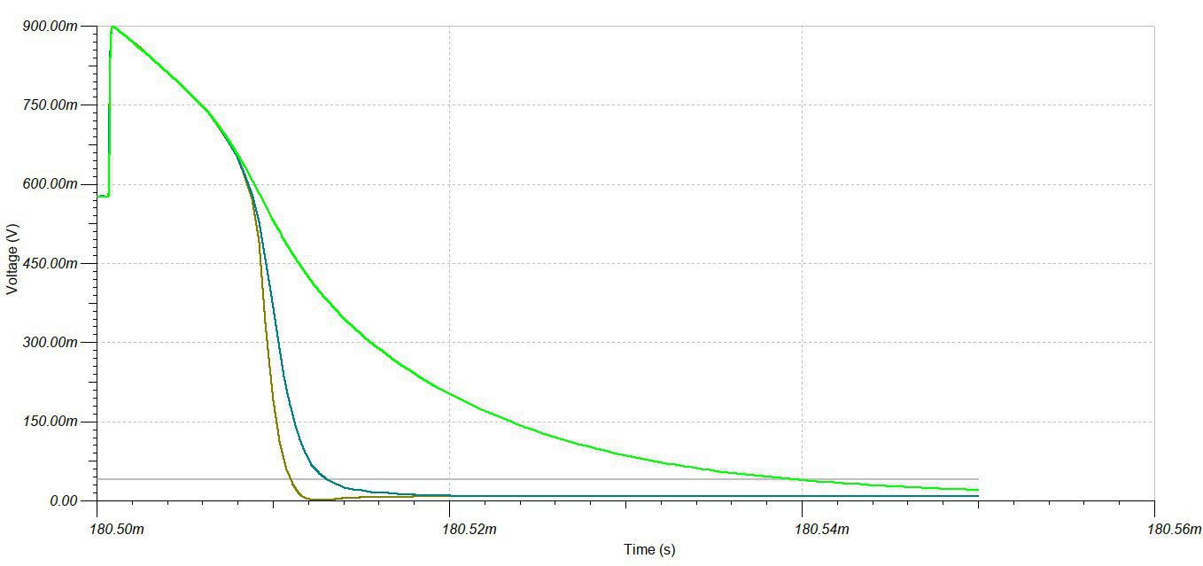
Low Pass Input Filter
I added a 1nF capacitor (blue curve) to signal input (brown curve). This has minimal impact on the signal but filters out any RF above 100kHz. For a 10kHz low pass filter (green curve) the capacitor would be 10nF but it materially delays the decay of the coil signal.
 Noise Floor
The noise level of the analog comparator is not disclosed in the ATMEGA328 data-sheet but if I use a 741 OpAmp as a model (23nV/sqrt(Hz)), the noise floor for a 100kHz bandwidth and 1k source resistance, will be about 7 uV.
Reducing the bandwidth to say 10kHz would reduce the noise floor to 2.3uV. At the moment the noise floor is not important.
Adding Gain
I don't want to use a split power supply OpAmp to avoid the extra power supply. So let have have a look at the LM324:
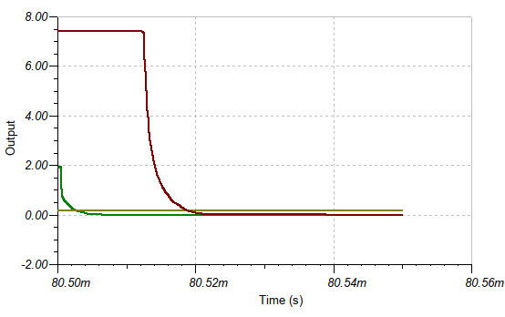
Note: the LM324 is DC coupled and has a gain of x20:
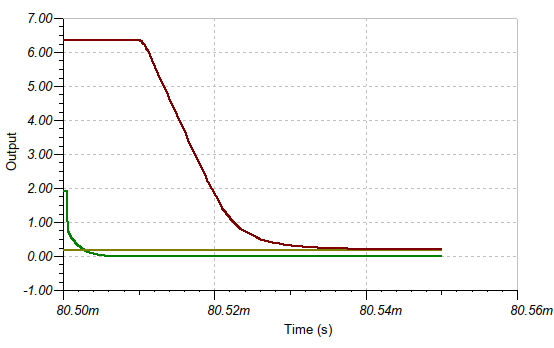
What you can see here is that the slew rate of the LM324 is far too low (the straight line descending slope) to follow the signal. This is not too surprising as the GBW of the LM324 is 1.2 MHZ and the slew rate just 0.5v/us.
Compare this with the LM3900 Norton OpAmp with a gain of x50:
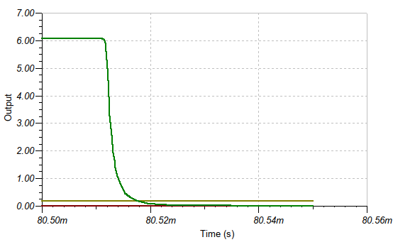
The LM3900 has a 4 MHz GBW and a 20v/us negative slew. But this is about as much gain as you can get with this OpAmp. Here is the lm3900 schematic:
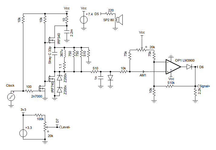
Note the common mode biasing using the 2x75k ohm and 20k Ohm trimmer. The common mode biasing ensures that the OpAmp has sufficient biasing to the inputs to operate correctly. It was a rather tricky design process to work this out.
The output diode drops the output offset from ~200 mV to 0 mV.
Another option is to use a CA3130, it has a slew rate between 10 and 30 v/us and a GBW of 15 MHz. For more gain (per stage), a more modern OpAmp such as the OPA365 is required:
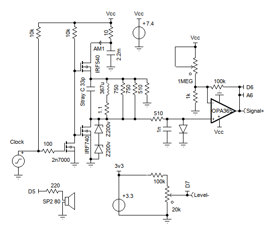
This OpAmp is rated at a GBW of 50 MHz and a slew of 25 v/uv:
Note the OPA365 was configured for a gain of x100 but higher gains are possible (x500 per stage).
Pseudo Gain Control
For signal processing it would be nice adjust the signal gain to normalising (i.e. make the start of the the signal the same voltage). This makes removing the ground response (i.e. subtracting the reference signal) more efficient.
While not ideal, we can initially set the analog comparator to the internal 1.25v reference. Start the signal timer at that point, and then measure the time for the signal to decay to the external analog comparator voltage reference (e.i. 40 mv). It is not the same as normalising the signal as there is a time shift but I suspect it will work okay in practice.
Digital Signal Processing (DSP)
I am near the end of what can be done with the analog input comparator. For the next PCB board I will connect the signal input to A5 as well as D6. Then I can explore ADC options and more advance DSP.
New PCB
So I am ready to design a new PCB.
AlanX
Discussions
Become a Hackaday.io Member
Create an account to leave a comment. Already have an account? Log In.