 Eric Hertz
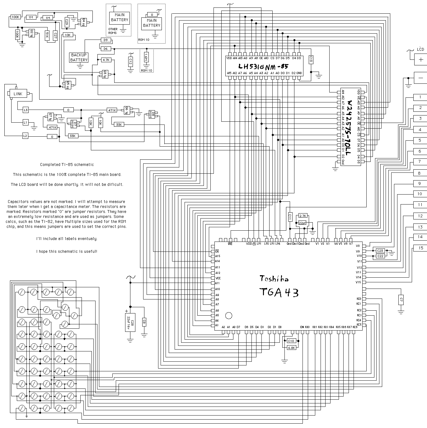
This is the alleged TI-85 schematic from https://www.ticalc.org/pub/text/hardware/
I have found some definite differences in my TI-86...
I'll get to those somewhat randomly.
Here's an oddity: BOTH the RAM and ROM have their Output Enables pulled low (active) at all times. The RAM's is handled through some diode-stearing with the backup battery which seems kinda odd in that it seems if the regular batteries are removed, it pulls the /OE low through two shottkey diodes, dropping ~0.7V. Is that "high" with the 3V battery? Or, maybe the ChipSelect is what matters, in that case, duh.
Ok, here's another, then... /ChipEnable seems to be tied directly to the processor... Same with the ROM. So, first, it would seem address-decoding logic splits out one address bit in both forms, active-when-high AND active-when-low, on two separate outputs, as both active-low. This could've easily been done with an inverter. Thus, I'm theorizing that the two otherwise unknown pins right next to them, on the processor, are actually Two More chip-select outputs, for two devices which aren't attached, and, then, Port 5 and 6 which use one bit to select between RAM and ROM (bit6) actually use bits 6 and 7 to select between FOUR different devices. Each up to 256k, with 16k banks.
This is further suggested by some key differences between the TI-85 schematic and what I'm seeing, here. EG on the 85 the processor's "/OE" is tied to the ROM's OE, but on the 86 it's tied to A16 on both the RAM and ROM. A17 to the ROM goes to the next CPU pin, unused on the 85.
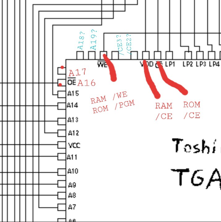
So, my guess is there are 18 address lines accessible to the outside, and four chip-selects (which would be two more address bits) so, twenty address bits, total.
Now, that'd be something! Though, there may even be more(?) The memory-mapping ports 5 and 6 would still have two unknown bits, 5 and 4. So it's maybe even possible there are two more address bits, currently unused, before the chip-selects. Haven't quite wrapped my head around whether that still fits within the memory-mapping...
The other oddity about the chip-enable being tied directly, in the case of the RAM, with its OE always active is that the /WR pulse must come *before* the chip enable. Maybe that's normal? OE is overridden by Write?
...
There was another oddity, which could be beneficial... even though the ROM in here is in fact a high-voltage OTP PROM, its /Program pin is actually connected to /Write-Enable along with the RAM... Looks like maybe they were forward-thinking to add FLASH (or used FLASH during software devel).
Discussions
Become a Hackaday.io Member
Create an account to leave a comment. Already have an account? Log In.