 Aleksa
The time had come to make a new prototype, one with all the hardware needed to accomplish the goals of this project! The front end was well proven at this point, and just needed a slight shrink to fit under an off the shelf RF shield. The ADC had always behaved well during my tests, but it needed a new (and untested) clock generator since the one I had prototyped with wasn't suited for it. Most disturbing of all, I needed to design with an Artix-7 FPGA and DDR3 RAM in BGA packages for the first time.
Tackling that last point first, I saw way too much risk in putting these BGA parts down on one board that I hand stencil and reflow solder on a hot plate. Not just that, but I only had three months until I had to submit this project to graduate my electrical engineering program and had no experience working with DDR3 nor even large BGA packages. I committed to learning these skills for the next revision, but had to find something to tide me over in a hurry.
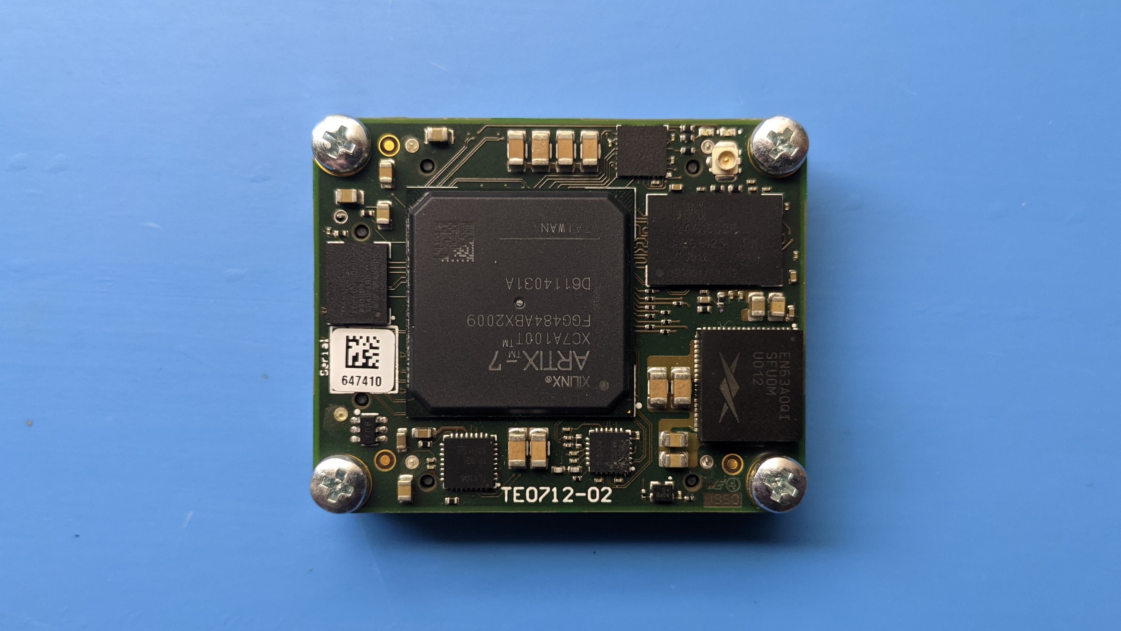
Enter, the TE0712-02 FPGA module. This bad boy had two DDR3 ICs, the second largest Artix-7 part, and only needed a 3.3V rail to operate. As my favorite circuits professor put it, "Simplicity itself".
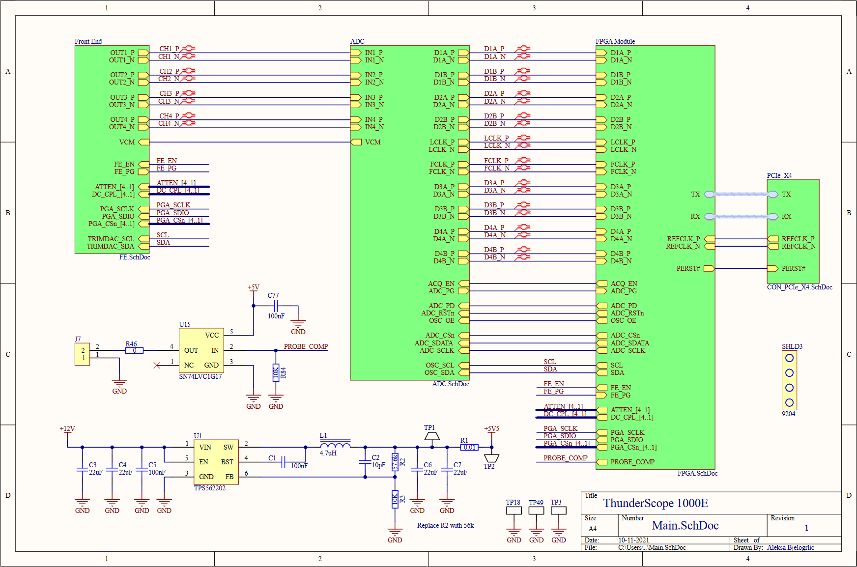
The top level of the schematic serves as a good block diagram for the entire prototype. The four front end outputs go to the ADC to be digitized, and the data and clock lines carrying the sample data are connected to the FPGA module, which also takes in all the control signals for the board. The FPGA module also connects to a standard PCIe x4 edge connector, which I used a project template to generate along with the specific board shaped needed to comply with the PCIe mechanical specifications. I included the PCIe mounting bracket (SHLD3) as a BOM (bill of materials) only part (not soldered on the board) so I don't forget to order it! I included a 74 series logic buffer (U15) to drive the probe compensation terminals (which I couldn't find the proper part for, so I just used right angle 0.1" headers) from the FPGA. PCIe has two power rails, 3.3V and 12V. The 3.3V rail is limited to 3A, so I decided to use the 12V rail to power the front end in case I drew too much current for just the 3.3V rail. To do this, I used a buck converter (U1) to step the voltage down to 5.5V, which was regulated to 5V with a linear regulator to reduce switching noise in the front end's power rail. I placed shunt resistors and test points on every regulator's input and output, so I can easily measure the current draw on each rail and the efficiency of the regulators.
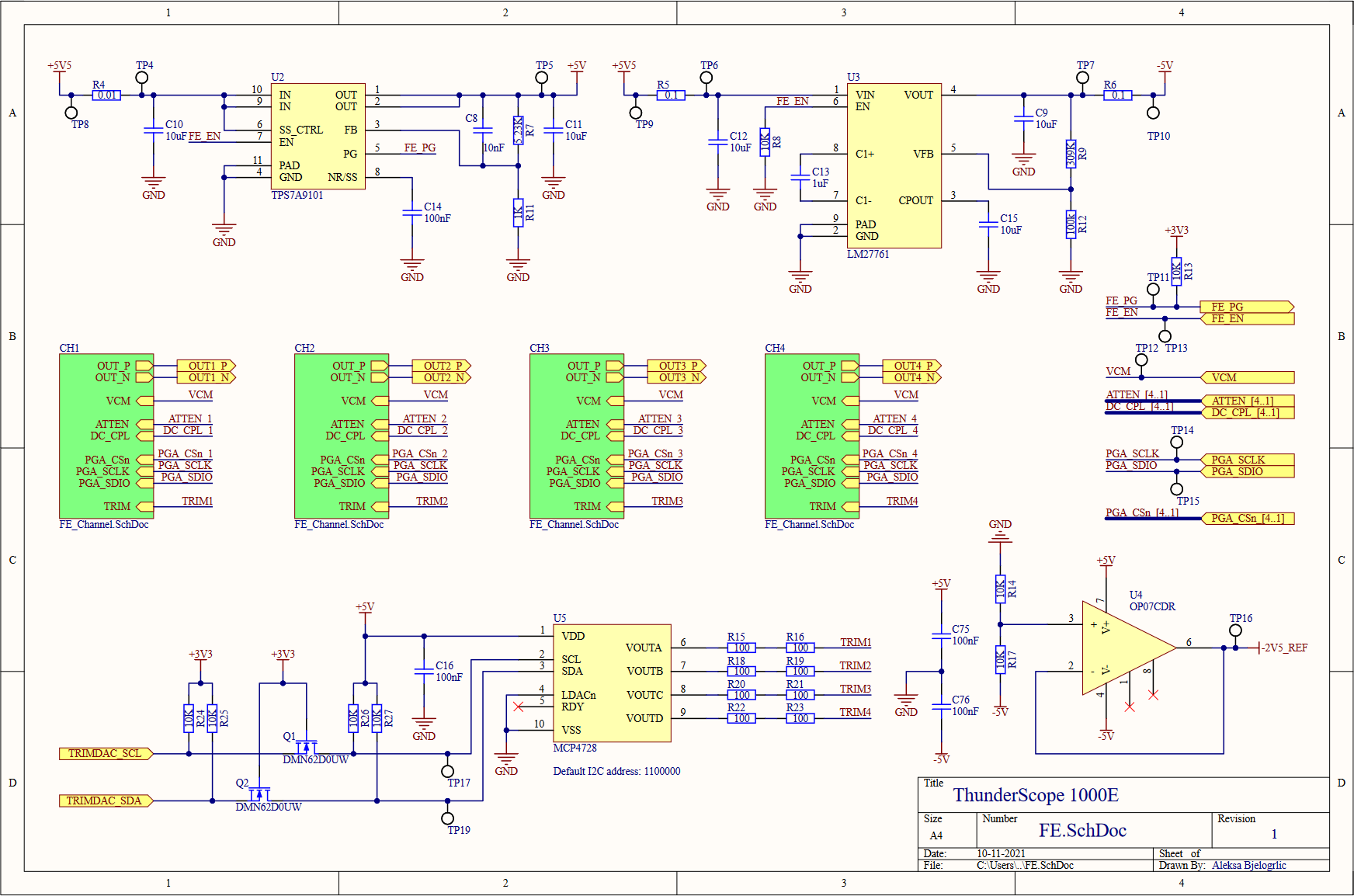
Moving on to the front end block, we see four front end channels, which will lead us deeper into this hierarchical rabbit hole. On the top of this sheet, we have the voltage regulation for the front end, both positive (U2, an LDO) and negative (U3, a charge pump with integrated LDO) 5V rails. A -2.5V reference for every channel's DC bias circuits is generated from this negative 5V rail using a divider (R14,R17) and buffered with an opamp (U4), this replaces the per channel divider from the previous design. A quad channel DAC (U5) is used to trim the DC bias values for each channel. This DAC is powered by (and referenced off of) the 5V rail, so it needed a level shifting circuit (Q1,Q2, and pull-up resistors) to match the 3.3V level of the I2C bus going to the FPGA. I also added test points on every signal going to the FPGA, better to be safe than sorry!
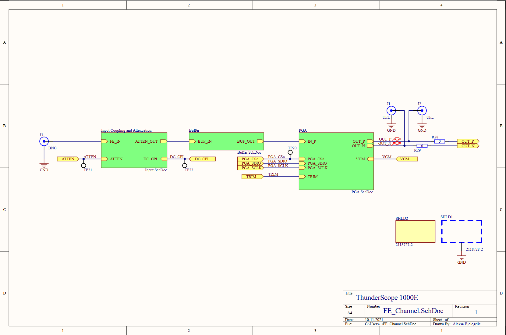
Last level of hierarchy before we get to the juicy stuff, I promise! On the left is the BNC input to the channel (J3), this is where the rubber meets the road (or where the scope meets the probe, ha). The RF shield I mentioned earlier comes in two parts, a frame (SHLD1) which is soldered onto the board, and a cover (SHLD2) which is press fit onto the frame. As with the PCIe bracket, I included the cover in the schematics and therefore the BOM so I don't forget to order it along with the rest of the parts. In order to test the front end channels, I included some UFL connectors (J1,J2) to bring the PGA output out as two 50Ω signals. When these connectors are used, the resistors (R28,R29) are removed to disconnect the output from the rest of the board to avoid doubly terminating the signal.
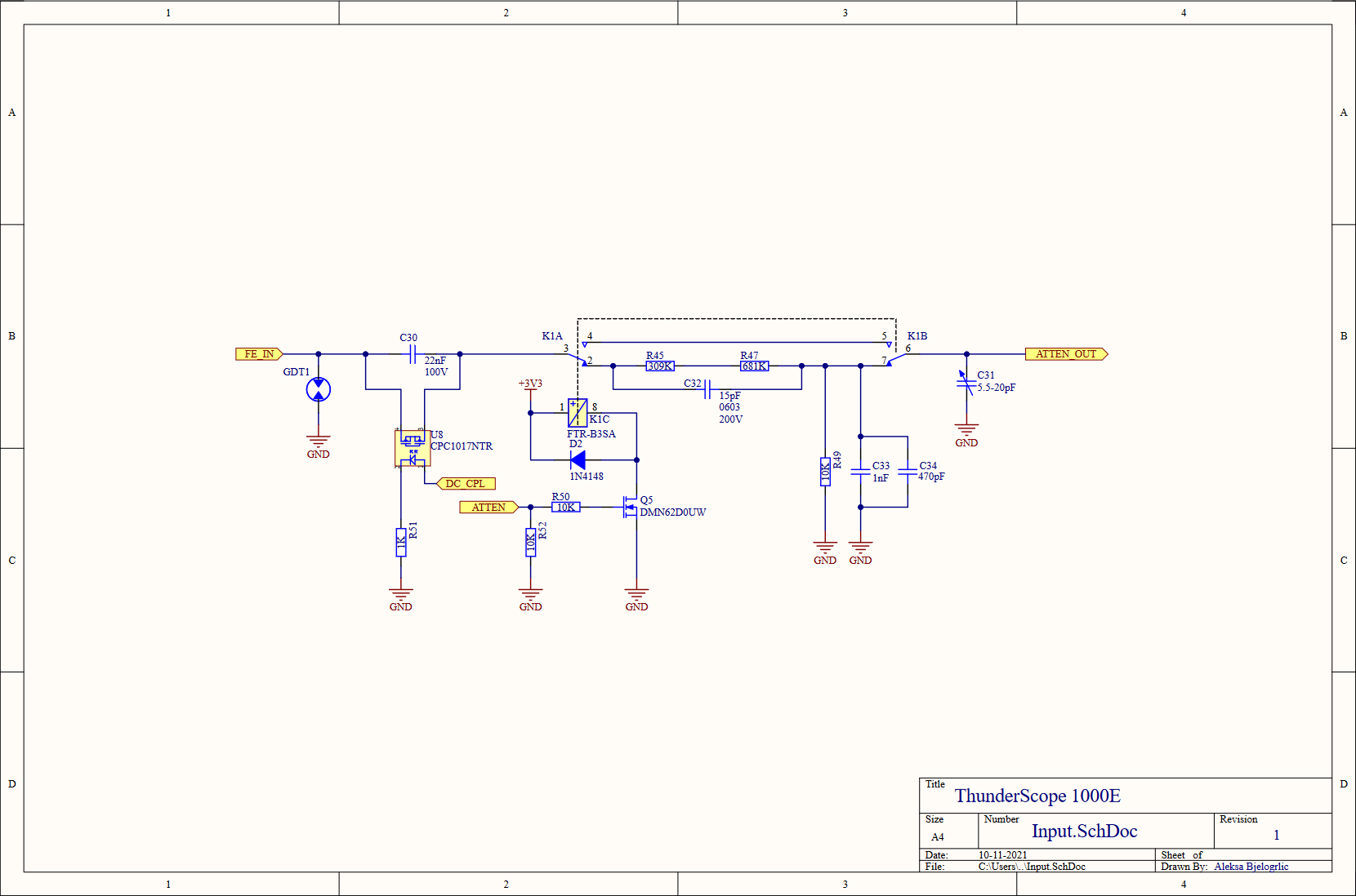
The input circuit was slightly simplified, removing the 6pF input cap right after the gas discharge tube and rolling it into the attenuator to get 15pF of input capacitance (provided by C32) when the relay is on. A variable capacitor (C31) was added to allow the capacitance on the non-attenuated branch to be changed to better match the attenuated branch. I also reduced the number of resistors in the attenuator, since it made no sense to worry about hitting an exact value when the resistors themselves have a 1% tolerance!
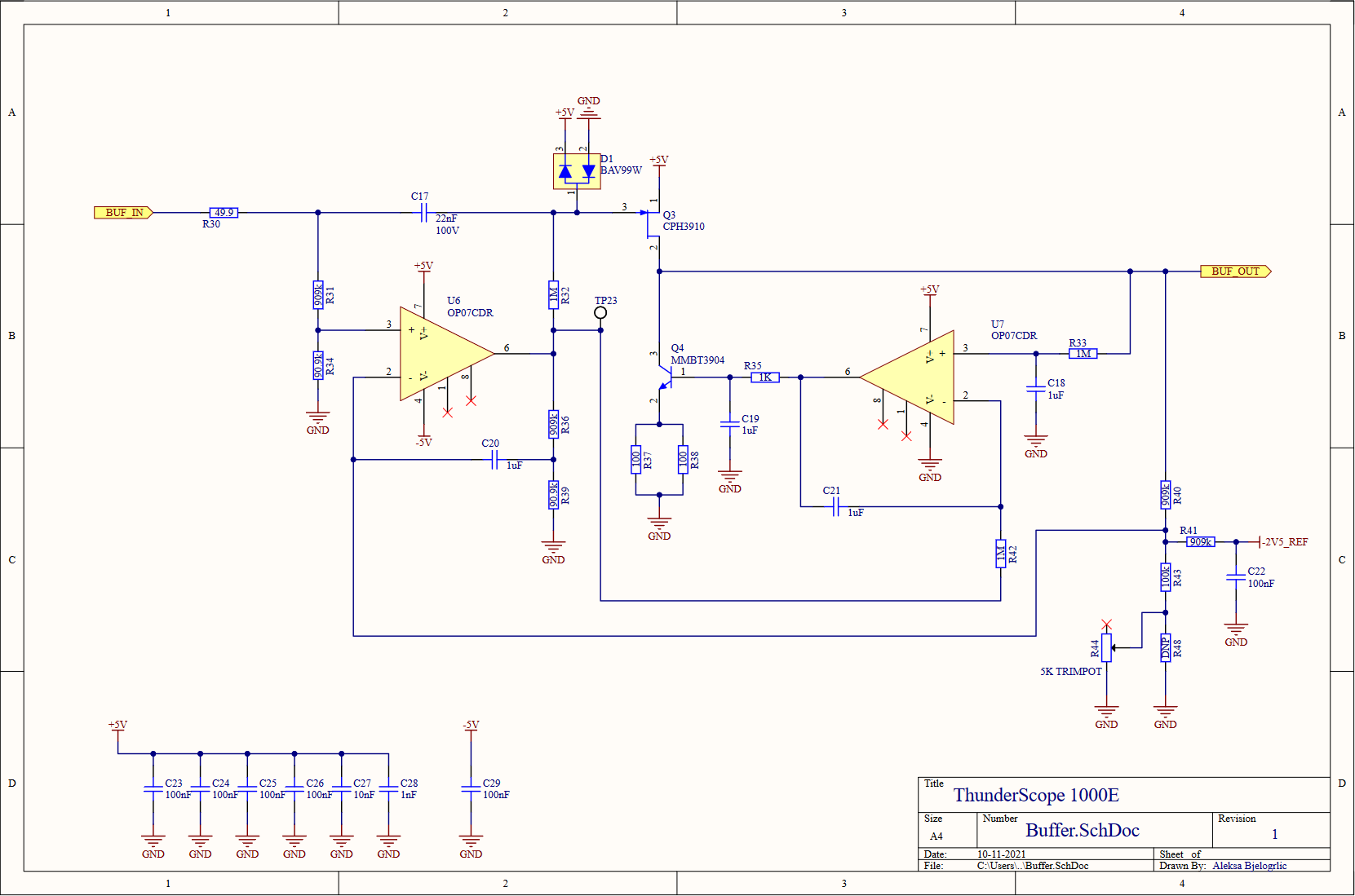
Continuing the trend of reducing the part count of this design, I replaced the two resistors that it took to get 900kΩ with a single 910kΩ, and replaced the 100kΩ that made up the other half of these dividers with 90.9kΩ to get the 1MΩ total (999.9kΩ, close enough!) needed. I also moved the protection diode over to the gate of the JFET (Q3) so that it wouldn't clamp on a DC over-voltage condition that the input would otherwise be able to handle (due to the divider on the opamp input, that node can handle up to 50VDC). I changed the value of R35 to 1KΩ from 3kΩ and C19 to 1uF from 330pF, using simulations to find common values to replace these values that didn't exist in the rest of the design. I did this to reduce BOM line items, which can reduce cost of assembly when going to a contract manufacturer. As a result of these changes, C20 also changed to 1uF from 100nF. I also split the 50Ω resistance at the emitter of Q4 into two 100Ω resistors (R37,R38) to better handle the 40mA maximum current flowing through it. Aside from using a buffered -2.5V reference, I added a trimmer potentiometer to the DC offset feedback divider to better tune the DC gain to match the AC gain of the circuit.
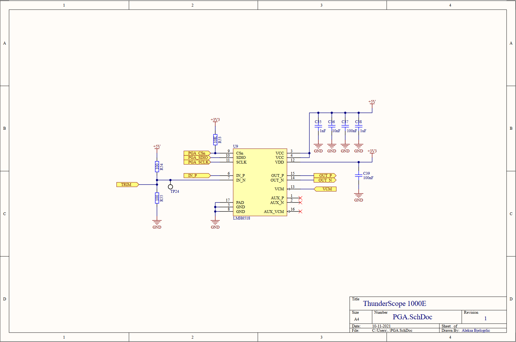
After that laundry list of a change log, I am pleased to tell you that nothing has changed in the PGA sheet. Better yet, we've completed our dive into the front end block. Now to resurface and explore the ADC and it's clock generator, which fit in just one page!
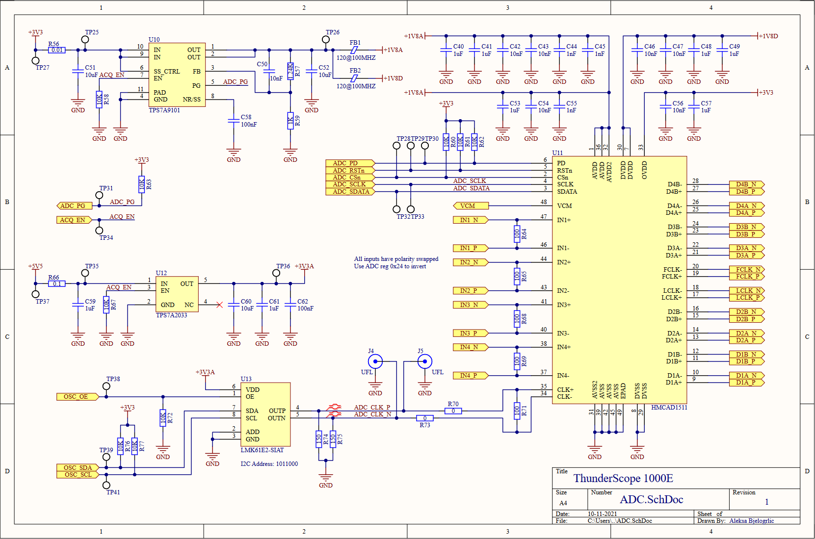
The hierarchy may be shallow, but this page wasn't smooth sailing! Luckily enough, not much has changed with the ADC or it's voltage regulation. The one major change was swapping the datasheet recommended input network to 100Ω resistors to terminate the PGA outputs properly.
The PLL I already prototyped with would provide very marginal performance as the ADC's clock, so I looked for something that would really make the most of the ADC. It needed to have low jitter, with a target to beat of 760 fs RMS measured from the previous circuit. To drive the ADC optimally, it also needed to have a LVDS or LVPECL digital differential output. I also wanted the simplest solution I could find to minimize the chances of this failing, since I likely wouldn't have time to make a new revision of this board by the capstone project deadline (so I was minimizing the chances of ME failing as well!).
In came TI to my rescue (a sentence not repeated since the start of the component shortages) with a wonder-chip. The LMK61E2 (U13) includes its own reference oscillator and loop filter, can output LVPECL, is configurable via I2C, and has a typical RMS jitter of 90 fs! This amazing chip cost almost twice as much as the previous solution, but it was a small price to pay for something that was almost sure to work. The almost in that sentence is why I included UFL connectors to pipe in a clock from somewhere else, or more optimistically, measure the clock generated by this chip. The LVPECL output requires a specific termination scheme, I used the convenient LVDS-like termination (R71,R74,R75) described in page 9 of this Renesas app note. I also added local regulation (U12) for this part to ensure a noise-free 3.3V rail, as opposed to the main 3.3V which is taken directly from the host PC (or Thunderbolt enclosure!) through the PCIe connector.
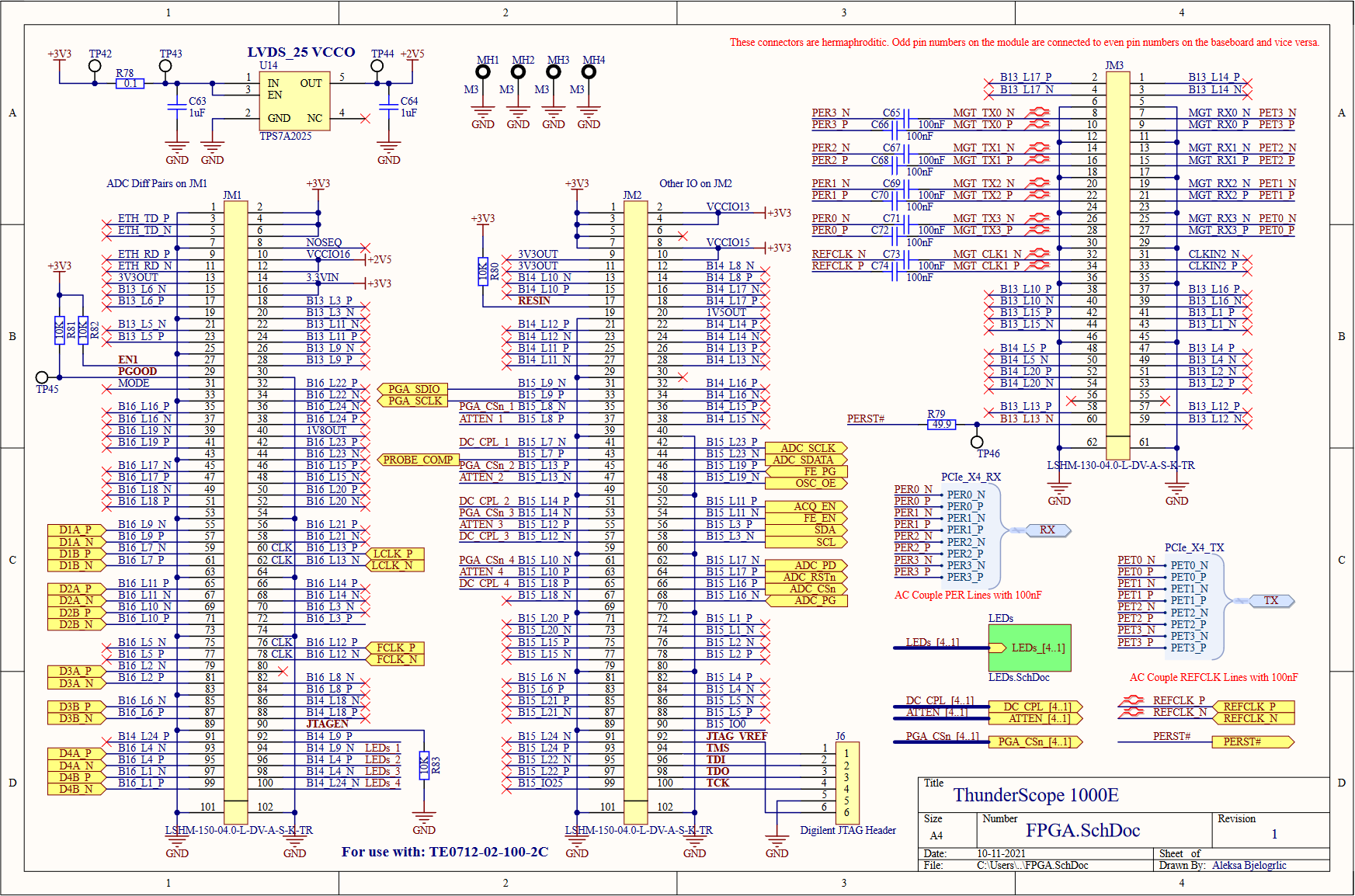
All roads lead to Rome and all connections lead to the FPGA! The FPGA module has three Samtec LSHM connectors which bring out the FPGA's IO banks and their voltage rails. All the bank IO voltages are set to 3.3V except bank 16, which must be 2.5V (regulated by U14, an LDO) to enable on-chip termination for LVDS. I brought the JTAG lines out to a header (J6) that matches the pinout of my programmer and included four LEDs (on a seperate page to save space) for debugging.
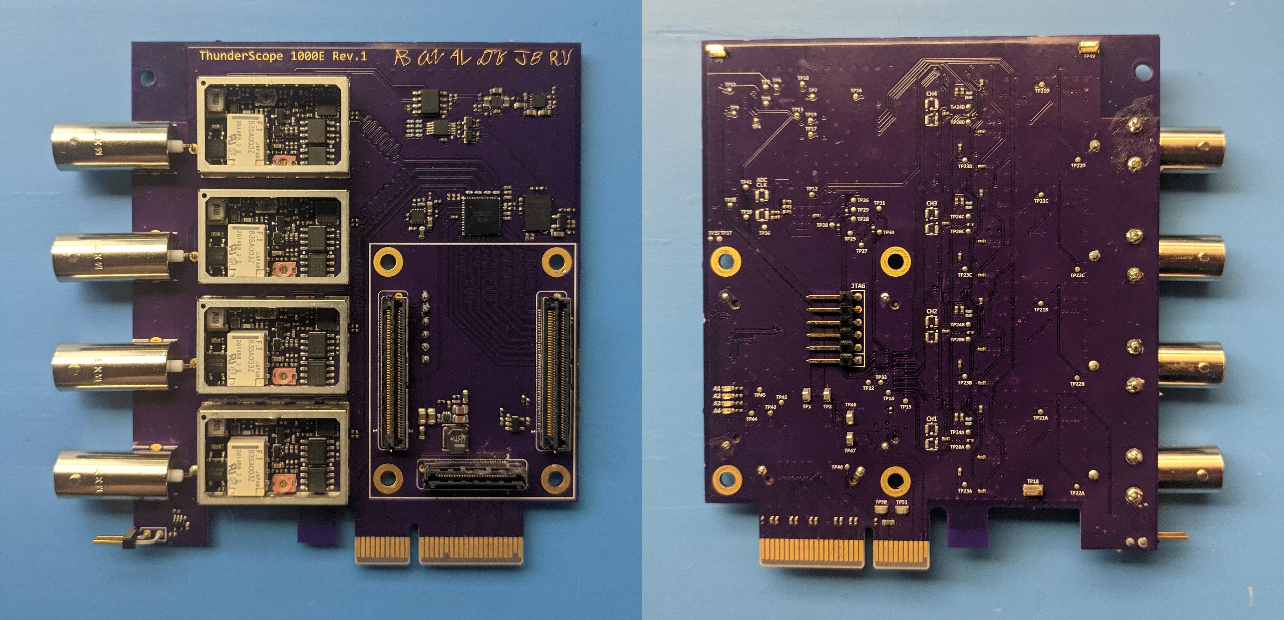
Here's how all of that looks on a board! I decided to get fancy with it and digitized my group members initials to include in an ENIG gold finish. And speaking of, what kind of software magic did the rest of my group get up to? Stay tuned for the next posts, which will be all about the software that makes this thing tick!
Thanks for giving this post a read, and feel free to write a comment if anything was unclear or explained poorly, so I can edit and improve the post to make things clearer!
Discussions
Become a Hackaday.io Member
Create an account to leave a comment. Already have an account? Log In.
We are very much interested in this version of Thundersope. We will be an early customer when it comes out. Have you ever tested the 1GSPS output of the ADC.
Can Artix handle such speeds?
Are you sure? yes | no
Glad to hear that! This ADC is particularly well suited for lower cost FPGAs since it uses 8 lanes of lvds @ 1 gbps each instead of one or two very fast ones. This way you can feed them straight into the FPGA instead of using the dedicated transceivers, as any pin on the Artix is capable of 1 gbps using the serdes primitive. We've tested this method and it works very well with minimal logic usage!
Are you sure? yes | no
Is the plan still to make this a thunderbolt device? I love reading these updates, i get excited when the pop up in my feed :)
Are you sure? yes | no
Glad to hear you enjoy them! Thunderbolt is still the plan, though I'll have to work with Intel to get the datasheet for their thunderbolt chip. I also plan on supporting USB 3 Gen 2 or USB 4 when an IC is released for it, which hopefully won't require an NDA!
Are you sure? yes | no