Lauri Pirttiaho
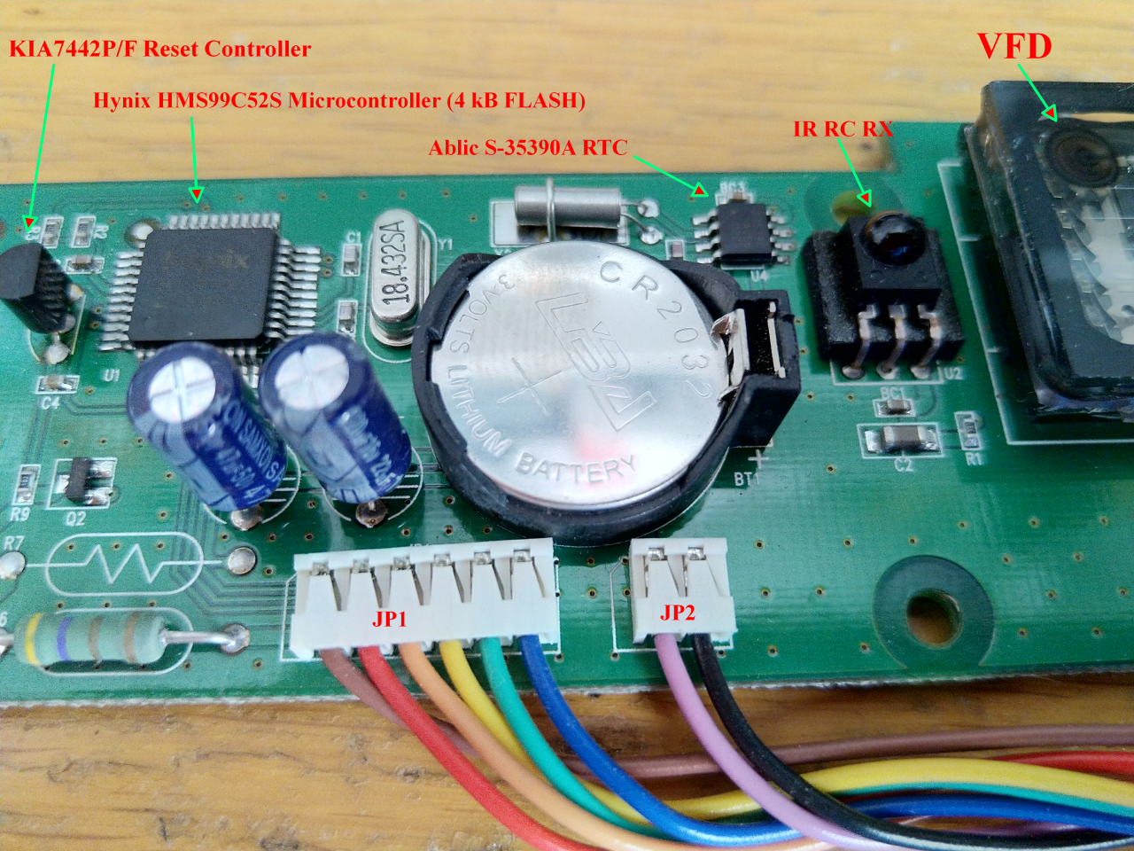
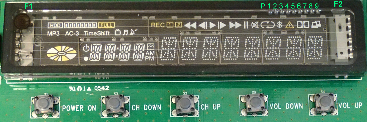
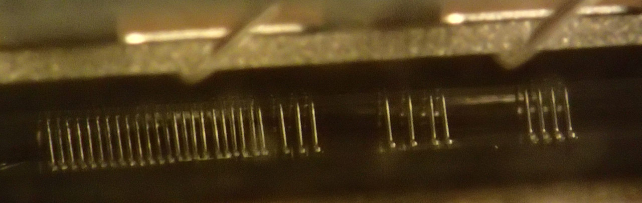
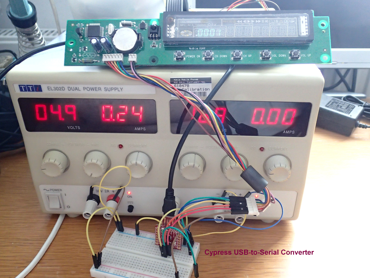
Connectors
- JP1
- Brown: Vcc (+5 V)
- Red: TXD (UART data from UI to main board)
- Orange: RXD (UART data from main board to UI)
- Yellow: GND
- Green: Connected to microcontroller T0/P3.4 (Indication from the UI module to the main board, low = power on, high = power-off)
- Blue: VFD HV (+17 V) - Connected to JP1-1 (Purple)
- JP2 (This is not needed. JP1-6 can be used for the VFD HV).
- Purple: VFD HV (+17V)
- Black: GND
The Vcc pin takes about 250 mA. The VFD HV pin takes about 9 mA when all segments are on.
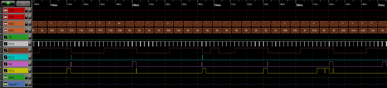
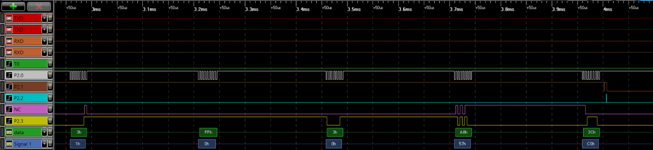
Protocol
The UART settings are 19200 baud 8N1.
The communication appears to consist of <STX> <type|dlen> <data>{dlen} <ETX> packets where type is the high nybble of the second byte and dlen its low nybble giving the number of data bytes following it.
Writing to Display
Messages of type 9 are used to write to byte arrays that the on-board microcontroller uses to drive the VFD.
Message 0x02 0x9<len> <addr> <data_0>...<data_len-2> 0x03 writes the data bytes to array at the given address. Each of the three multiplexed data sets are 16 bytes long. Set 0 is at address 0x00, 1 at address 0x10, and 2 at address 0x20. Since one write is limited to 14 bytes of data the main board CPU writes each set with two writes: first 8 bytes to 0x[0-2]0 and then 8 bytes to address 0x[0-2]8. The first data byte of each set (0x[0-2]0) selects the grid and it is 0xC0, 0x3C, or 0x03 for sets 0, 1, and 2, respectively. The set 1 appears to contain largest number of segments and is probably for that reason allocated 4 outputs, while two other sets use 2 outputs. The rest (120) bits select the segments (1 on, 0 off)
Mapping of the segments
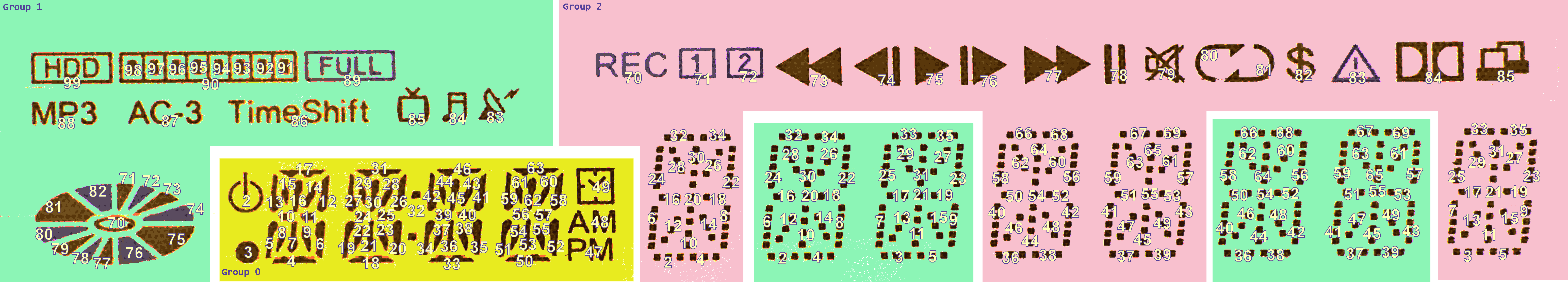
Zoom into the image to see the set (grid group) and segment mapping. Note that segment numbers map to bits in the messages so that bytes 0-6 are in the first message for the set and bytes 7-15 in the second. Bits are numbered so that msb is 0 and lsb is 7. Byte number is the segment number divided by 8 and the bit number is the remainder of the segment number when divided by 8.
Simple Display Driver
A display test program with a simple driver class is in tf5100ui-vfd-test.py
Special Display Controls
The display can be controlled also with shorter messages than full groups. The message 0x91 is special so that it can be used to clear the display (0x02 0x91 0x00 0x03) or it can be used to set groups of segments (like 0x02 0x91 0x01 0x03) up to turning all segments on with 0x02 0x91 0xff 0x03.
After clearing the display the bytes driving the grids (0x00, 0x10, and 0x20) have been set correctly. Then one can write to all other bytes or ranges of bytes any segment driving values with 0x20 0x9<L> <addr> <value>+ 0x03, where L is number of bytes -1, addr is the address of the first byte and value-bytes give the patterns (+ indicates like in regexp one or more values).
Real-Time Clock
The time from the real time clock can be read with message 0x02 0x10 0x03. The device responds with 0x00 0x02 0x13 <hr> <min> <sec> 0x03.
The whole real-time clock calendar can be read with message 0x02 0x30 0x03. To that the device responds with a 5-byte data that contains year, month, day, week day, hours, minutes, and seconds. The message looks like 0x00 0x02 0x25 <year[6:0]|month[3]> <month[2:0]|day[4:0]> <weekday[2:0]|hours[4:0]> <minutes> <seconds> 0x03. The year is 0..99, month 1..12, day 1..28..31 depending on month and leap year, weekday 0..6, hours 0..23, minutes and seconds 0..59.
This same message can be sent to the device to set the real-time clock to any allowable value. Incorrect dates appear to be adjusted to the next valid one. The device responds with 0x00 0x02 0x30 0x03.
If the real-time clock battery is dead the response to 0x02 0x30 0x03 is 0x00 0x02 0x15 ... (time response 0x1L , not calendar+time, 0x2L) with the calendar data invalid (year 101, month and day both 6, or other garbage), but the time is valid, counting up from the power-on.
The data sheet of the chip mentions that it has auto-calendar up to...
Read more »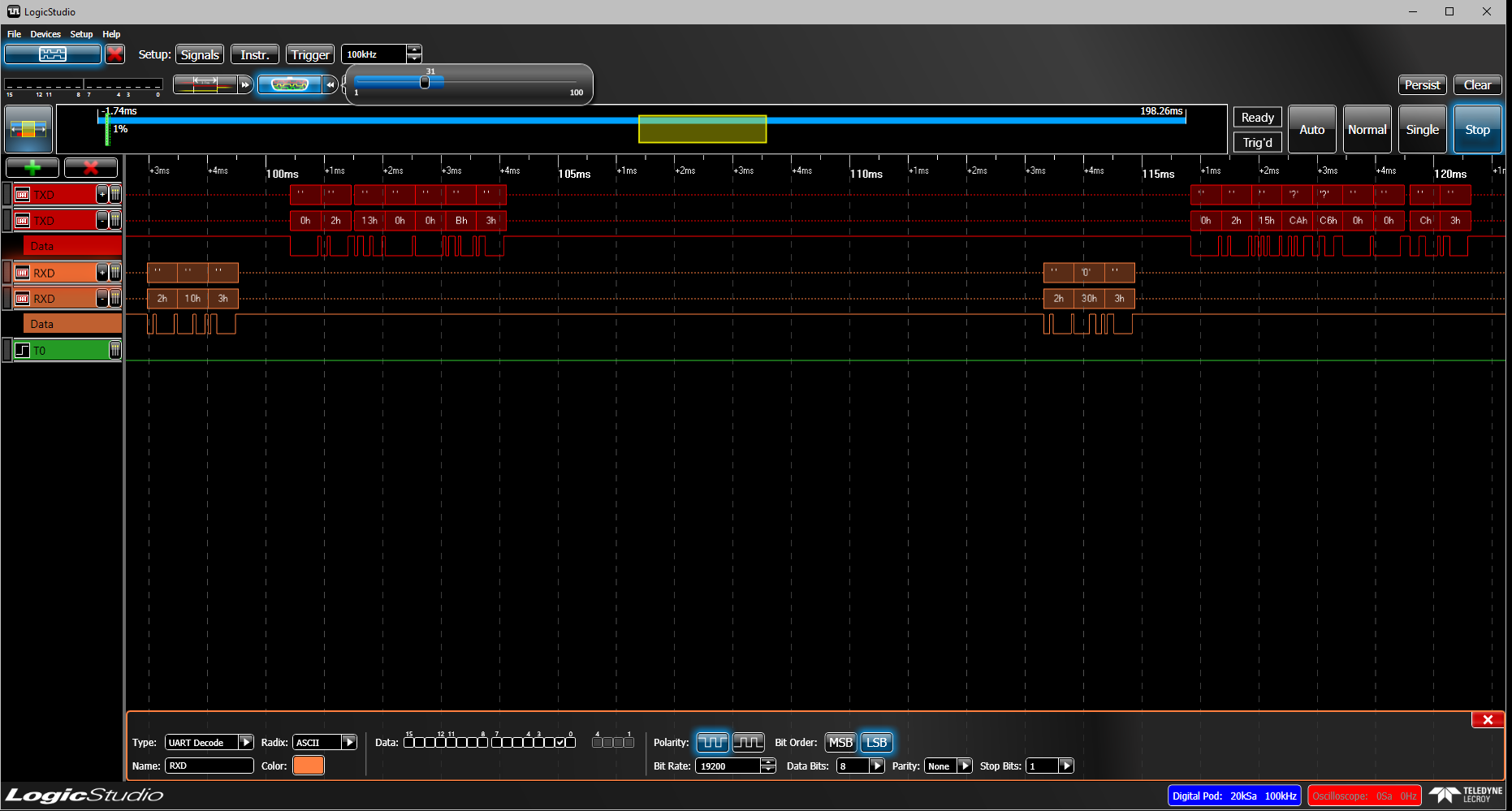

 Mike Szczys
 Gee Bartlett