David H Haffner Sr
UPDATE 01/12/2018 6:31:PM
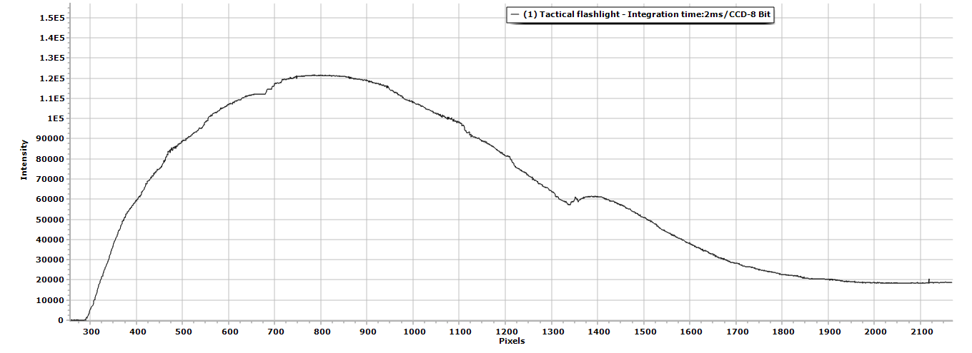
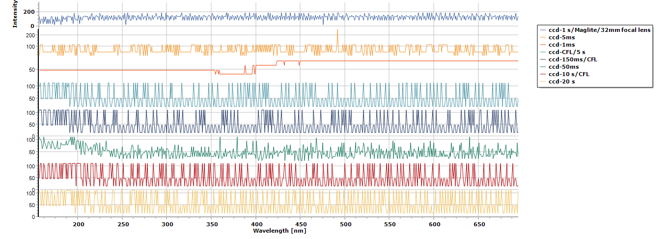
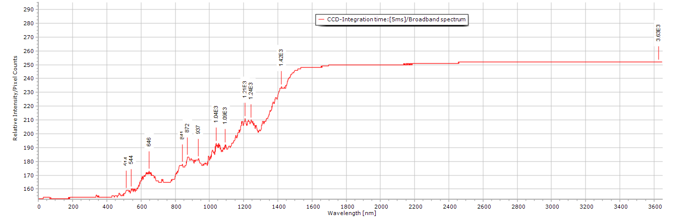
Tactical flashlight scan @ 2ms CCD 8-Bit (TCD1304DG) detector circuit test:
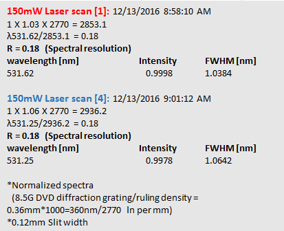
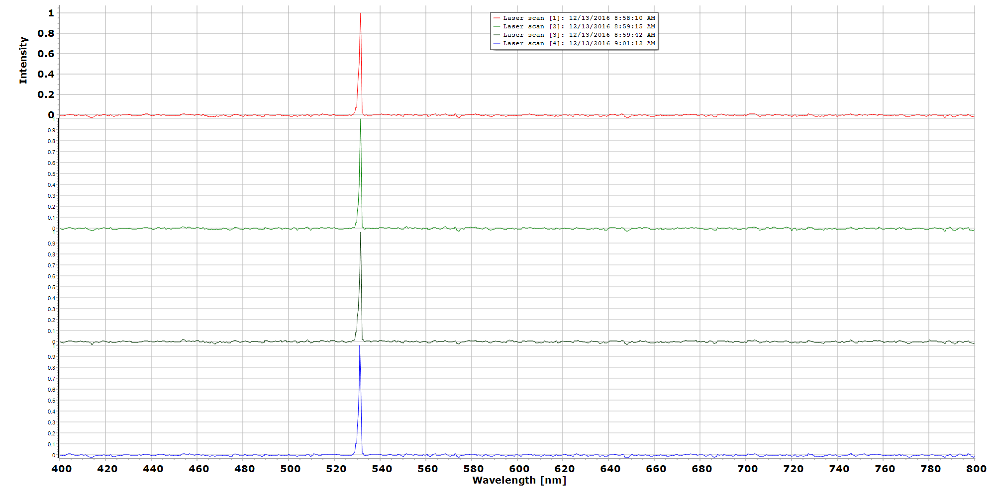
A better 1st mirror alignment and a 2nd 150mW laser line test:
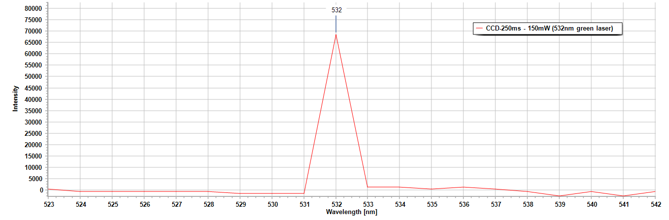
The plot above has a FWHM value of 1.005nm resolution.
Fixed the 1st mirror position, I have much better resolution now :)

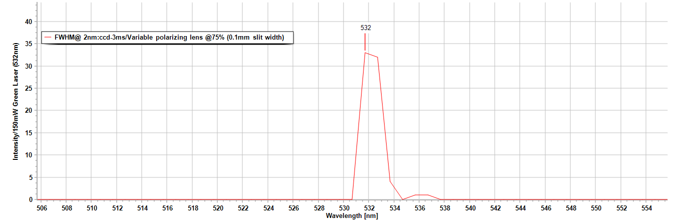
Another test scan today using my Aries 150mW green laser and a 0.1mm slit width @ 3ms integration time:
A little bit of clipping can be seen even though I had the variable polarizing lens at 75% still got a resolution factor of 2nm :)

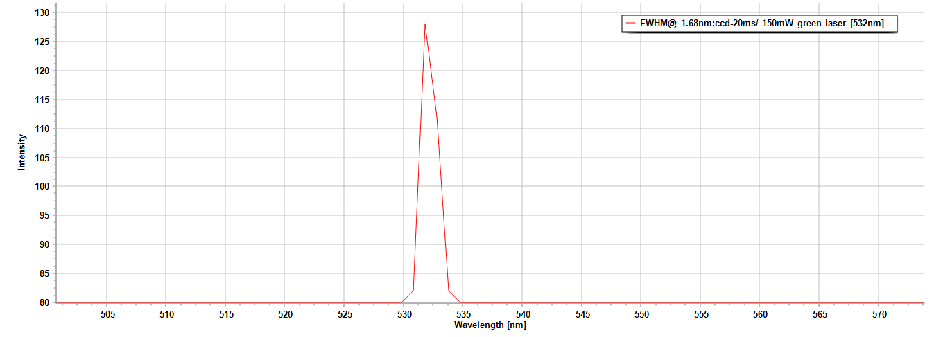
New test scans using the 8-Bit CCD detector (TCD1304DG)
Final version of the Motor Control Targeting Interface unit for the diffraction grating turret control system:
Excel chart data:
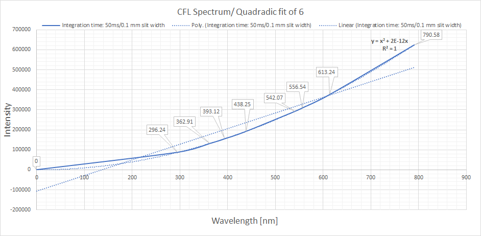
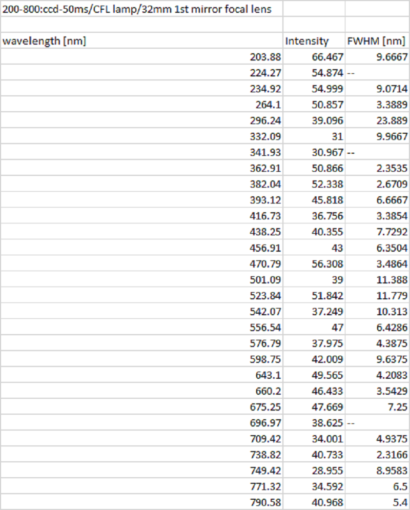
New CCD scans using a 32mm achromatic coated lens @ the 1st collimation mirror and a compact fluorescent lamp, below is the raw data of various scans:
Below is the processed data of my CFL lamp:
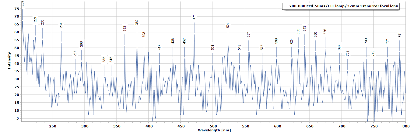
and finally, the FWHM data from the above spectrum:
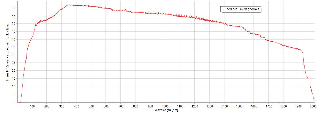
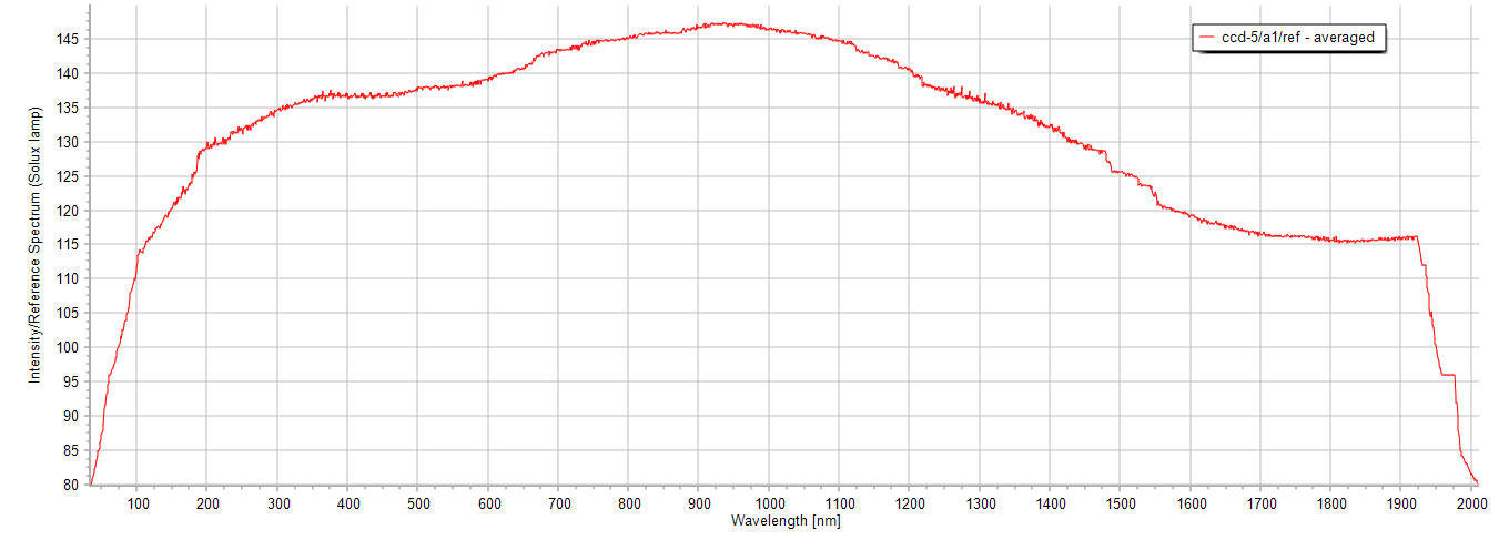
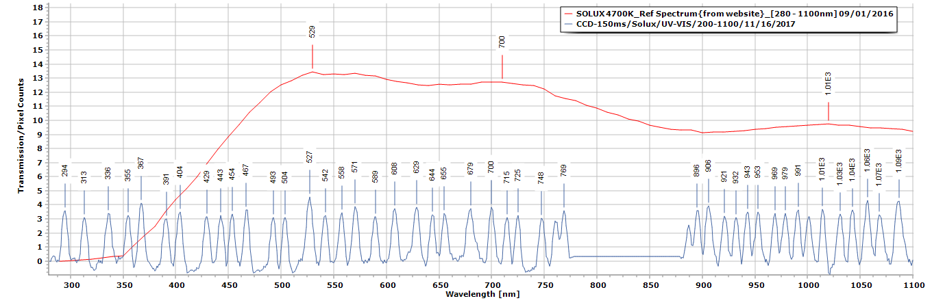
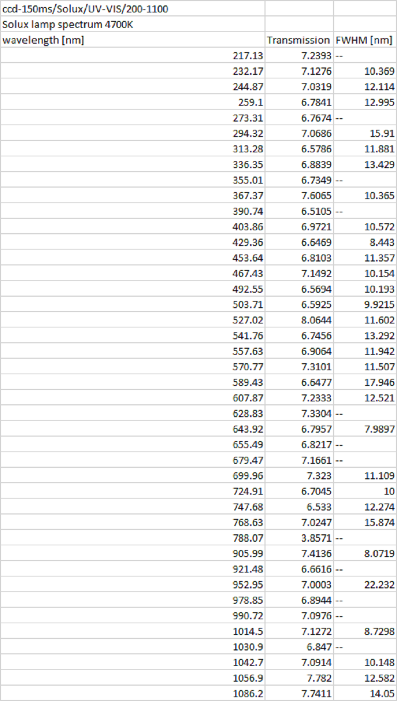
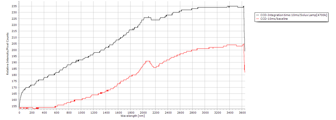
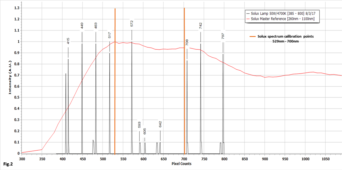
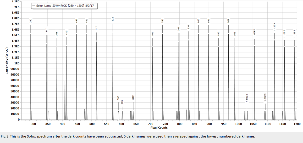
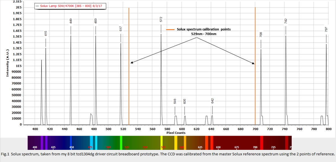
A calibrated Solux lamp spectrum (mine,) 4700K/50W/12vdc/1.2A/0.10mm slit width
Turret @ zero position (baseline) 0.00 nm/ Integration time: 150ms
2400ln/mm diffraction grating:
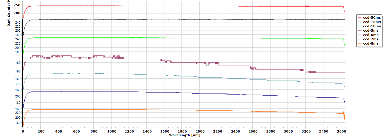
7 Dark Count scans I did to determine which integration time is the most ideal and it appears to be 50ms, 15ms and 10ms:
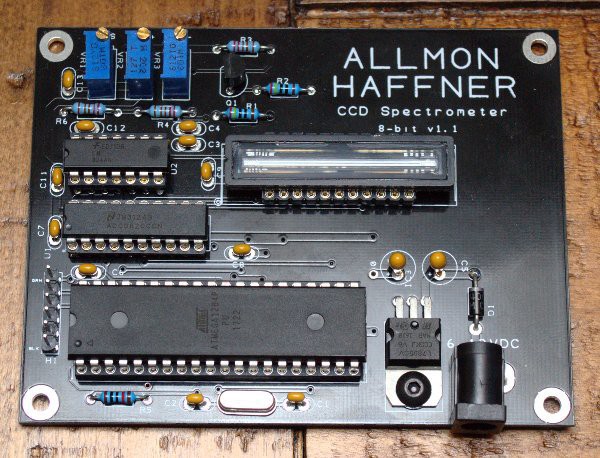
CCD detector Allmon & Haffner v1.1 is done.
-Testing Platform
PLX-DAQ v2.11 Dual Trace Transfer to Excel
New 8-Bit TCD1304 CCD detector driver board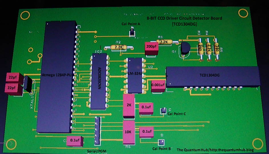
New schematic
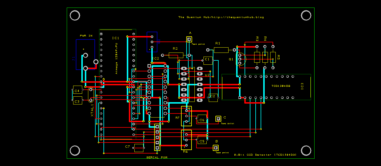
8-Bit Main SCH 1
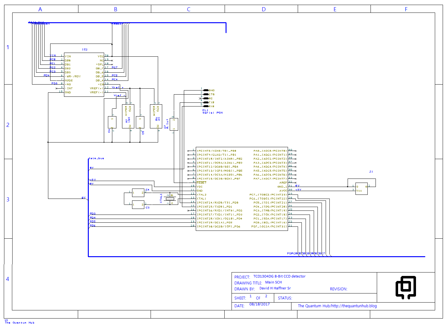
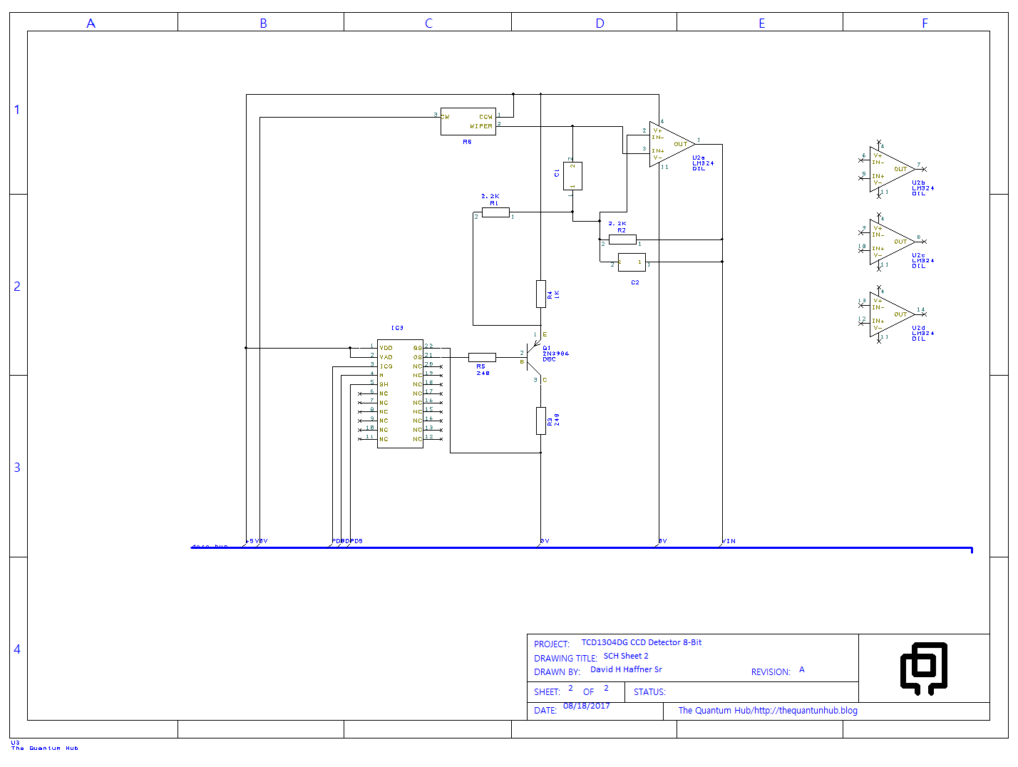
8-Bit Sheet 2
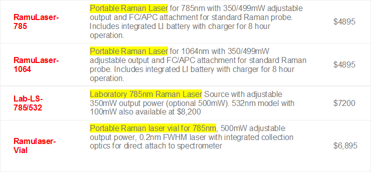
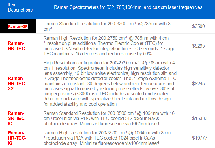
Cost analysis comparing Raman Spectrometers and Lasers from StellerNet Inc. to the DAV5 V3.01 3D printable Raman Spectrometer:
DAV5 V3.01 Raman Spectrometer uses an Aries 532nm 150mW CW/DPSS Green Laser
Cost - $ 199.99 US
The DAV5 V3.01 3D Printable Raman Spectrometer
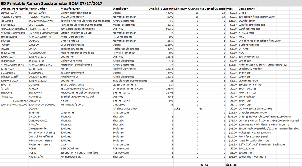
DAV5 V3.01 Raman Spectrometer - $ 657.35 US
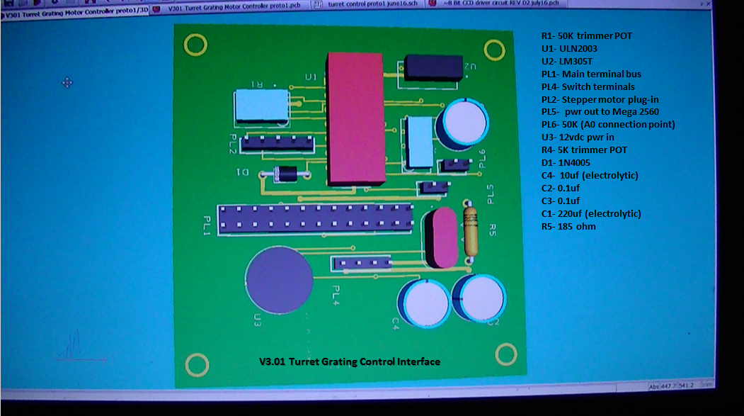
Here is the 3D view of the turret control interface unit for controlling the stepper motor, which turns the diffraction grating mount inside the spectrometer.
2 new spectral images today using a 0.1 mm acetate (film) slit, I allowed only 2 mm in length, of light to pass through the monochromator.
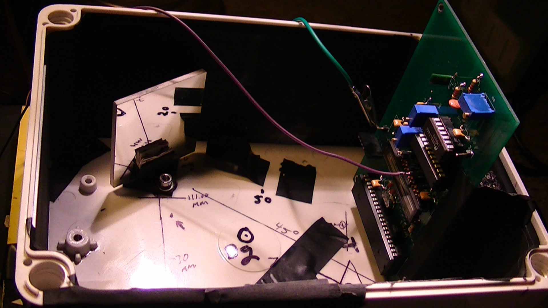
I cleaned the CCD noise up a bit and readjusted R4 and R7, and it certainly made a big difference, also the significantly narrower slit width makes a difference too.
The values for R4 and R7 are approximate for the breadboard, since the runs are longer than they would be on a PCB, but this gives me a great calibration starting point when the circuit is put together and ready for testing.
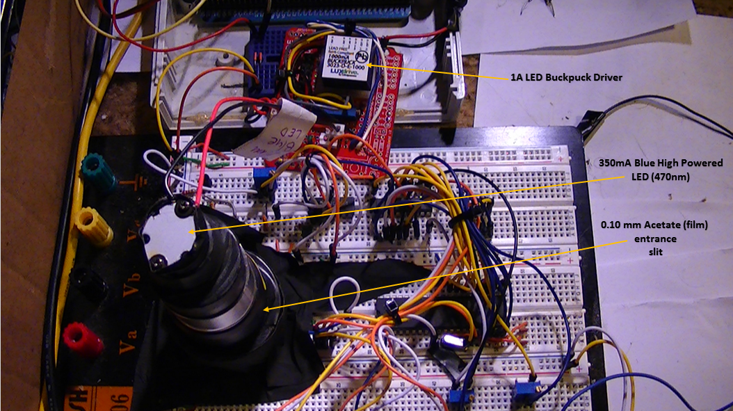
As you can see in the above image, the entrance slit is a rig I designed about a year and a half ago.
New CCD Spectrograph Hardware and Software
7/13/2017
This unit captures all of the TCD1304's 3648 pixels using the ADC0820 8-bit half-flash converter. The time to digitize a frame is 32mS. At 115.2kBaud it takes a couple of seconds to download a frame.
Hardware
An ATmega1284 was chosen as the microcontroller. It has 16kB of RAM, which is double the Arduino Mega2560. The sensor is the Toshiba TCD1304AP, a 3648 pixel linear CCD sensor which operates on a single voltage (3.0V to 5.5V). The sensor is driven directly by the microcontroller, and the analog output is buffered by a transistor and an op-amp. The signal is digitized by an AD0820 analog to digital converter.
The ADC0820 has + and - reference inputs, and this design takes advantage of them. A pot is used to set the maximum range of the ADC, and another pot sets the minimum range. In this way you can tune out the unused portion of the range and get all 256 values from the ADC.
The things that set this spectrograph apart from the last one are its ability to read all 3648 pixels from the CCD, and read them faster than the previous version. Because the AD0820 is so fast, I was able to tighten the code up and get all of the pixels read in 32mS. It reads 3694 pixels, but the first 30 and the last 16 are dark reference or dummy pixels and are discarded.
The Mclk signal has increased from 380kHz to 470kHz on this version.
Reference;
http://davidallmon.com/pages/adc0820-spectrograph
The firmware can be downloaded here: Arduino CCD 8 Bit Driver Firmware
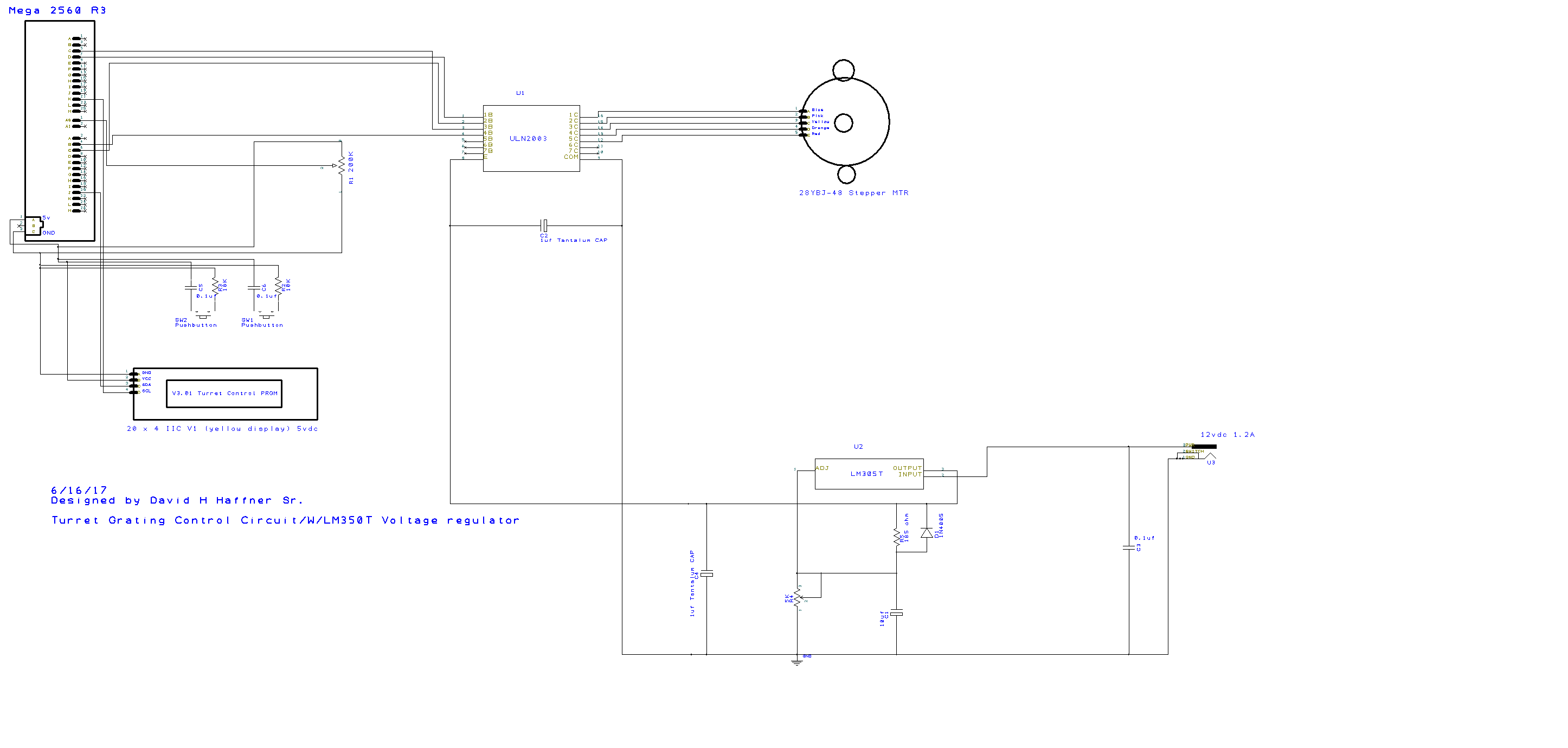
Stepper program for the 28YBJ-48 (stepper MTR) and degrees step
/64
Speed is controlled by a delay between each step.
The longer the delay the slower the rotation.
That delay value is obtained by reading and analog-to-digital
cover (A0 in this case/10K trimmer POT) which gives a value from
0 to 1023.
The value is divided by 4 and add 10 for a delay
in milliseconds:delay(analogRead(0)/4 +10)
For faster speeds change 10 to say 2.
This is calculated between every step to vary speed while stepping.
I incorporated unsigned long int Val, in order read a little bit more of the AN/Map
A nice feature of unsigned int's: if a val is unsigned, then val / 4 is optimized by the compiler into a bit shift, much more efficient than the actual division you would get if val was signed.
Highlights of this code:
1) NO debouncing program
2) NO external Stepper lib
3) NO PWM
4) unsigned long int val = (analogRead('...') / 4 + 2); if a val is unsigned, then val / 4 is optimized by the compiler into a bit shift, much more efficient than the actual division you get if val was signed.
5) Push button control incorporates 2 functions per switch;
1: momentary push & release = Start/Stop
2: press & hold = Continuous operation
I have run several tests using my Atmel 1284P Development Board and the data transfer protocol is working perfectly :)
*UPDATE* 5/1/2017 11:23AM
I had to make a revision to the firmware for the ATmeg1284P driver software, it's in a zip file at Github, same link below "
I rewrote to firmware on AtmelStudio 7.0 and uploaded the files to a new repository at my Github website, so it's all nice and tidy :) Here is the repository; http://github.com/dhaffnersr/AtmelStudio-7.0
*UPDATE* 4/29/2017 3:55PM
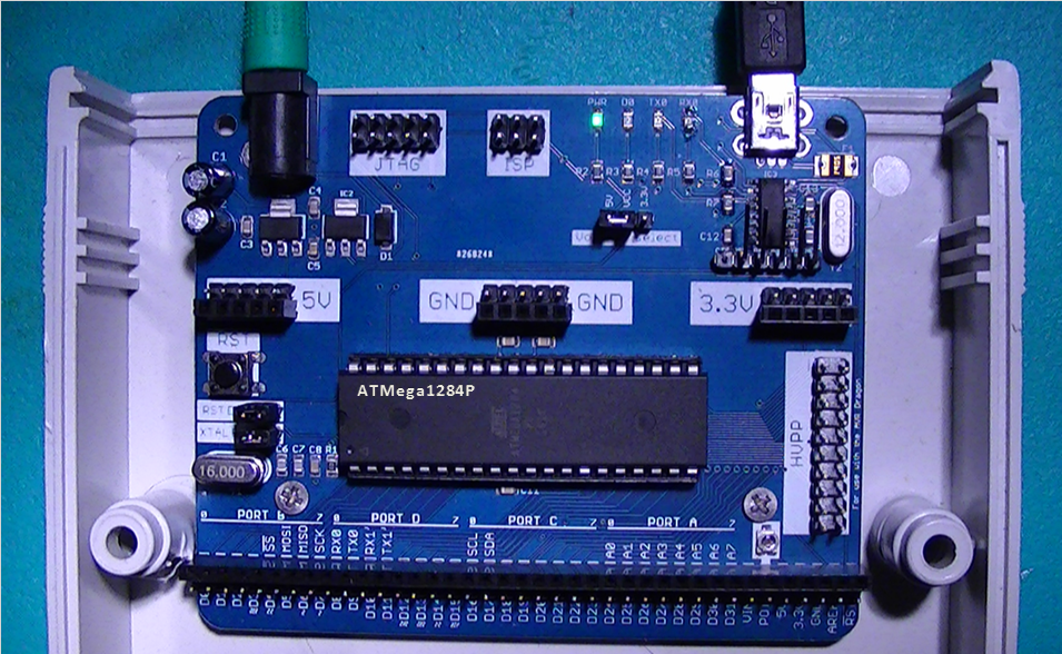
This is the development board that I use from MCUdude over at the Tindie.com store, not only is this thing versatile, but lets me switch between different 40 pin chips, which of course right now I am using the ATMega1284P. One in the CCD detector circuit board and here in this Dev board.
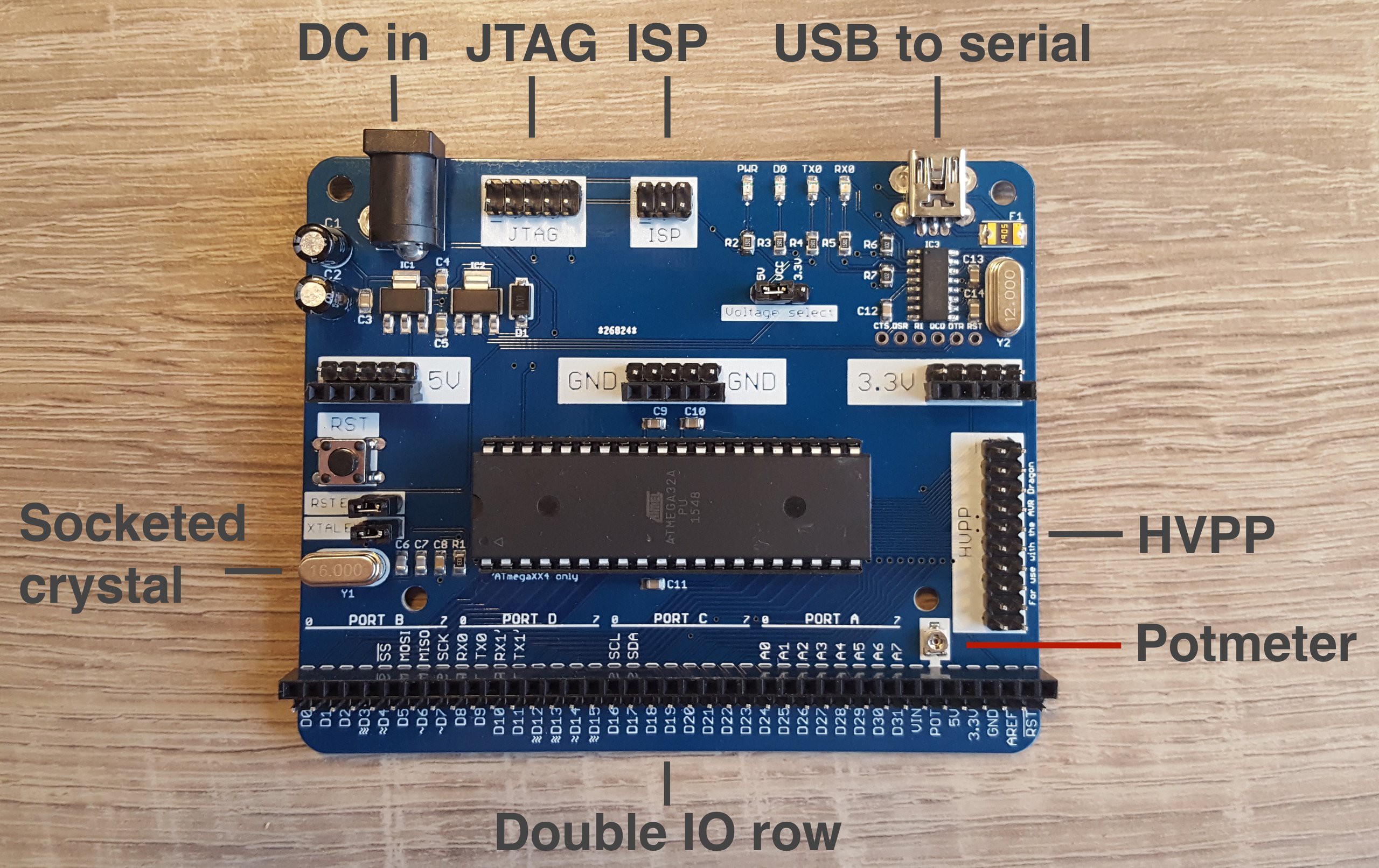
This is my board with the ATMega1284P chip;
This is my projects MISSION STATEMENT:
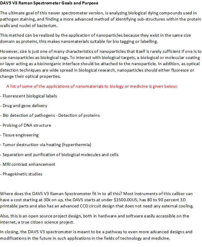
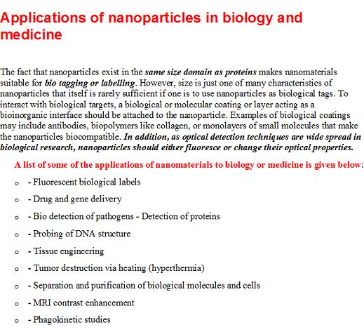
This is the primary motivation for doing this project from its inception over a year ago to present day, I specialize in biological pigments and dyes. This is the ultimate direction that this project will be moving toward. Nanoparticles used as bio tags for an unprecedented level for cellular targeting eliminating the need to use the conventional methods of bio staining.
Reference:
http://www.ncbi.nlm.nih.gov/pmc/articles/PMC419715/
*UPDATE* 3/11/2017 4:55AM
The LS-532A-laser collimation tube assembly, is my design and build. I have assigned it this nomenclature for easy identification.
Here are the three components that will be a critical part of the CCD driver circuit, so I wanted to post a general feature and description of them, starting with the AD8021 opamp (which will be used as the pre amp for the ADC (AD7667)
GENERAL DESCRIPTION
The AD8021 is an exceptionally high performance, high speed voltage feedback amplifier that can be used in 16-bit resolution systems. It is designed to have both low voltage and low current noise (2.1 nV/√Hz typical and 2.1 pA/√Hz typical) while operating at the lowest quiescent supply current (7 mA @ ±5 V) among today’s high speed, low noise op amps. The AD8021 operates over a wide range of supply voltages from ±2.25 V to ±12 V, as well as from single 5 V supplies, making it ideal for high speed, low power instruments. An output disable pin allows further reduction of the quiescent supply current to 1.3 mA.
*UPDATE* 3/27/2017 5:54:AM
I eliminated the MAX232EIN from the circuit equation, it cannot handle the load placed on it from the AD8021 op amp, so it is going to be replaced by the MAX660 - Switched Capacitor Voltage Converter. The MAX660 CMOS charge-pump voltage converter is a versatile unregulated switched-capacitor inverter or doubler. Operating from a wide 1.5-V to 5.5-V supply voltage, the MAX660 uses two low-cost capacitors to provide 100 mA of output current without the cost, size and EMI related to inductor based converters. With an operating current of only 120 µA and operating efficiency greater than 90% at most loads, the MAX660 provides ideal performance for battery-powered systems. MAX660 devices can be operated directly in parallel to lower output impedance, thus providing more current at a given voltage. The FC (frequency control) pin selects between a nominal 10-kHz or 80-kHz oscillator frequency. The oscillator frequency can be lowered by adding an external capacitor to the OSC pin. Also, the OSC pin may be used to drive the MAX660 with an external clock up to 150 kHz. Through these methods, output ripple frequency and harmonics may be controlled. Additionally, the MAX660 may be configured to divide a positive input voltage precisely in half. In this mode, input voltages as high as 11 V may be used.
http://www.ti.com/lit/ds/symlink/max660.pdf
AD7667
FEATURES
2.5 V internal reference: typical drift 3 ppm/°C Guaranteed max drift 15 ppm/°C Throughput: 1 MSPS (Warp mode) 800 kSPS (Normal mode) 666 kSPS (Impulse mode) INL: ±2.0 LSB max (±0.0038% of full scale) 16-bit resolution with no missing codes S/(N+D): 88 dB min @ 20 kHz THD: –96 dB max @ 20 kHz Analog input voltage range: 0 V to 2.5 V No pipeline delay Parallel and serial 5 V/3 V interface SPI®/QSPITM/MICROWIRETM/DSP compatible Single 5 V supply operation Power dissipation 87 mW typ @ 666 kSPS, 130 µW @ 1 kSPS without REF 133 mW typ @1 MSPS with REF 48-lead LQFP and 48-lead LFCSP packages Pin-to-pin compatible with AD7671, AD7677
GENERAL DESCRIPTION
The AD7667 is a 16-bit, 1 MSPS, charge redistribution SAR analog-to-digital converter that operates from a single 5 V power supply. The part contains a high speed 16-bit sampling ADC, an internal conversion clock, internal reference, error correction circuits, and both serial and parallel system interface ports. It features a very high sampling rate mode (Warp), a fast mode (Normal) for asynchronous applications, and a reduced power mode (Impulse) for low power applications where power is scaled with the throughput. The AD7667 is hardware factory-calibrated and comprehensively tested to ensure ac parameters such as signal-to-noise ratio (SNR) and total harmonic distortion (THD) in addition to the more traditional dc parameters of gain, offset, and linearity. Operation is specified from –40°C to +85°C.
ALL Updated STL. mesh files for this project are also available at http://github.com/dhaffnersr/STL-mesh-files-FreeCad-0.16-/tree/freecad-v0.16
*New spectral resolution data:

*Scan LS-2A - 531.6/790 = 0.67nm / R = 0.67 (spectral resolution)
*Same scan will have an R value of 0.37nm spectral resolution when the new Holographic diffraction grating is in place ( it has 1800 ln/mm.) I wanted to be clear that the data above to the far left, shows what the R value would have been if the 1800 ln/mm grating would have been in place.
I will be adding more details as I move the project along, but for today I have uploaded the main 3D printable components, more to come.
ALL .STL mesh files that I upload are FREE to download for anyone, and get creative with, modify whatever, that is the spirit of what I do here!
Definition of: Raman spectroscopy (/ˈrɑːmən/; named after Sir C. V. Raman) is a spectroscopic technique used to observe vibrational, rotational, and other low-frequency modes in a system. Raman spectroscopy is commonly used in chemistry to provide a fingerprint by which molecules can be identified.
DAV5 V3; DVD diffraction grating (2770 lines per mm_8.5 G) Present slit width; 0.12mm
Cmos specs: 2 megapixels,1920x1080 JPEG video compression
Optical Resolution
The optical resolution of the spectrometer is determined by the input slit size and the optics inside the spectrometer. The best possible resolution that can be obtained is the diffraction limit, which is the resolution obtained with an infinitely small input slit. The diffraction limit is related to the size of the beam width inside the spectrometer. For instance, equation 3 determines how the beam width on the grating wbeam limits the resolution ΔλFWHM:
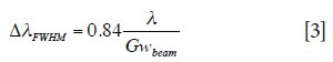
The wider the beam, the more grating lines the beam illuminates and, therefore, the better the resolution. This is also referred to as the resolving power of the grating.
Resolution
The resolution of a spectrometer defines the ability to resolve closely spaced features in the spectral domain (measured in nanometer or wavenumber). Raman spectra often exhibit closely spaced peaks and for this reason spectrometers with high resolution are required. However, the resolution will also influence the size of the spectrometer as will be explained in this section.
The resolution of the spectrometer is determined by the following two factors:
- Pixel resolution: The number of pixels covering the spectral range.
- Optical resolution: The image of the input slit on the detector.
- Pixel Resolution
· The more pixels the detector has, the better the resolution, as seen from the example in Table I. However, more pixels generally also mean a wider detector, which again means a larger spectrometer as explained previously. Because the smallest pixel spacing of scientific CCDs is typically in the 10–12 µm range, one can say—as a rule of thumb—that 2048 pixels corresponds to a 1-in. detector while a 512-pixel detector corresponds to a ¼-in. detector. Typically, a peak need to be sampled by a minimum of 2–3 pixels to determine the peak center accurately. Process Raman typically requires ~10 cm-1 resolution, so with a 1024-pixel detector (4.5 cm-1/pixel sampling as seen from Table I) we should be able to obtain the required resolution. If the resolution requirement is 20–25 cm-1, we can even reduce the number of pixels to 512. ![]()
- Spectral bandwidth/Specification data for the DAV5 V3 Prototype (a) Raman spectrometer;
![]()
- 150mW Aries DPSS Laser [532nm];
![]()
- Raman bands of interest in this project;
- The diffracted light of
interest is from 500-4000 cm⁻¹ in
the Raman spectrum, which with an excitation wavelength of 532 nm translates to
546.5-675.6 nm, because:
![]()
- Now that I will be utilizing a CCD detector, I will be able to expand my Raman signal range in the future utilizing a 785nm regulated laser source, although I will still be using the Aries 532nm CW green laser (150mW)