 Dave Collins
Introduction
It's interesting how these projects can take a completely different direction than when you started out. About 2 weeks ago I decided that this project had kind of a turn off the road, and the reason that happened is, in my mission to make the project as absurd as I possibly could I'd really set some design goals that should not have existed. I set out to see if I could make a CPU from op amps. If you know me, then you know when I set goals like that unless something else pops my interest I'll probably build a CPU from op amps... the only trouble was I'd greatly underestimated the size of that rabbit hole.
Building a digital CPU from what is essentially an analog competitor has consistently more variables and pit falls than traditional logic. Don't get me wrong, I work in telecom, I spend 8-13 hours a day looking at spectrum readings on a scope I am well aware of the analog component to digital signaling, I knew this would be difficult on the outset. What I did not understand going into this would be the time sink that this type of project would create... and for a while that was great I was definitely not bored, after all I like solving problems from data and signal readings I am a annalist.
Also, as I continued to prototype and build this thing up on the bread board it became clear that, though it would absolutely be possible to build a 1-bit CPU from op amps on a bread board; it was basically just a large state machine. Additionally, the more and more I built, the more I started to realize that at the end of this I was really excited for the state machine build. And with that excitement came the realization that I was simply delaying the project that I wanted to do in order to optimize the project that I was really just interested in for it's absurdity.
OPEN LOOP?
I get this question a lot. the answer is yes, when the op amp is in open loop its basically a really inefficient comparator. essentially when the voltage on the input side of the gate's input pin is less than the voltage at the divider on the opposed input pin the gate is in cut off, and when it is greater than the voltage at the divider it "rails out and registers a high signal (close to but not exactly the same as the VCC of the circuit. Also important to note the source voltage pins are tied to +12v and GND at the positive and negative input pins respectively. The High state on an open loop op amp is generally "good enough" to trigger another gate in a combinational logic setup.
The ALU Design
The turning point for me was running into Ken Shirriff's blog on the Z-80 ALU. Its an interesting read if you have the time (and its short so I highly recommend it!). He goes in to great detail the design of the Z-80 4-bit ALU. You heard that right, 4 bits ALU for a 8 bit CPU. He also lays out a very good explanation of the inner workings for the 1-bit calculation cell used on the chip for the 4-bit alu. It was so fun to read I thought i'd build it up in Logism:
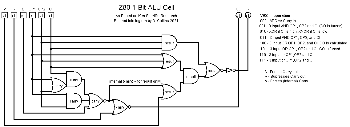
As you can see as simple as it gets; it has an 8 bit multiplexer built in ... and is so simple it relies on further logic to drive the inputs for 2 component comparison (it only has 3 way gates, and certain states must be asserted by the rest of the CPU to produce proper calculations). In fact, as I read, I became hooked on this design and thought it would be no problem to build it up on a bread board with op amps.

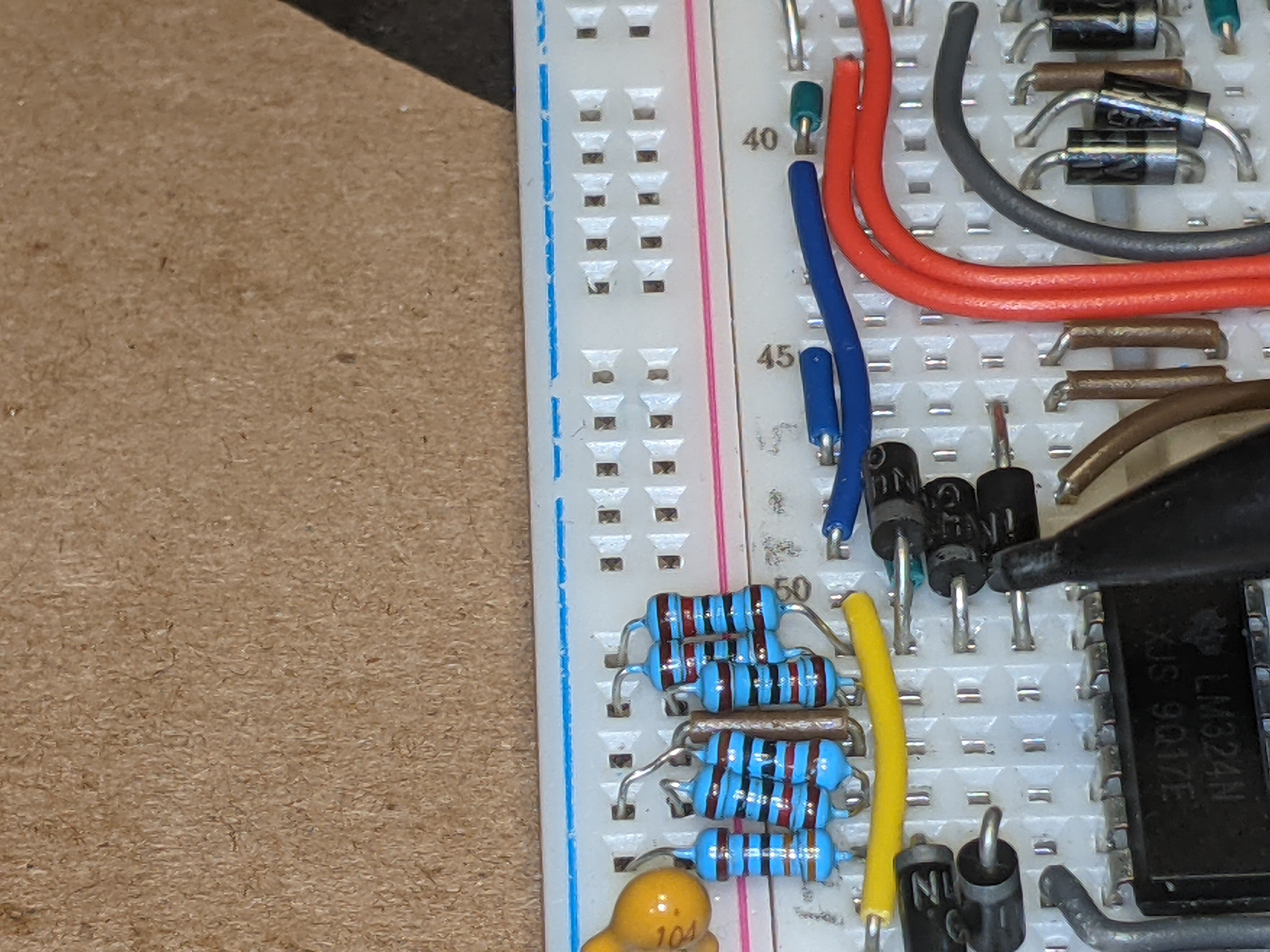
It probably took about another week to build this in afternoons after work, and then another two days to troubleshoot values to really get it working. But in the end I did end up with a fully functioning ALU:
It's an interesting little thing to play with; I'll be honest some times i just plug it in and push the buttons just to appreciate the absurdity of what is really going on here. But honestly to really understand it, I should break down how each gate type works:
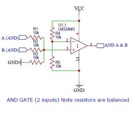
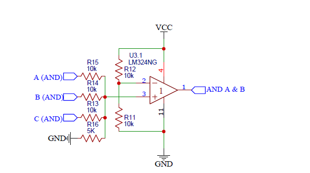
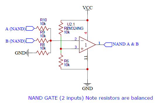
AND GATE
A and gate is built with only resistors and depending on the number of inputs, those resistor values will generally mostly be the same value. For my experiments I chose 10k but without going into too much of the math (and there are plenty of really good videos on the math involved with op-amps) that value seemed to work well with 12v for my VCC.
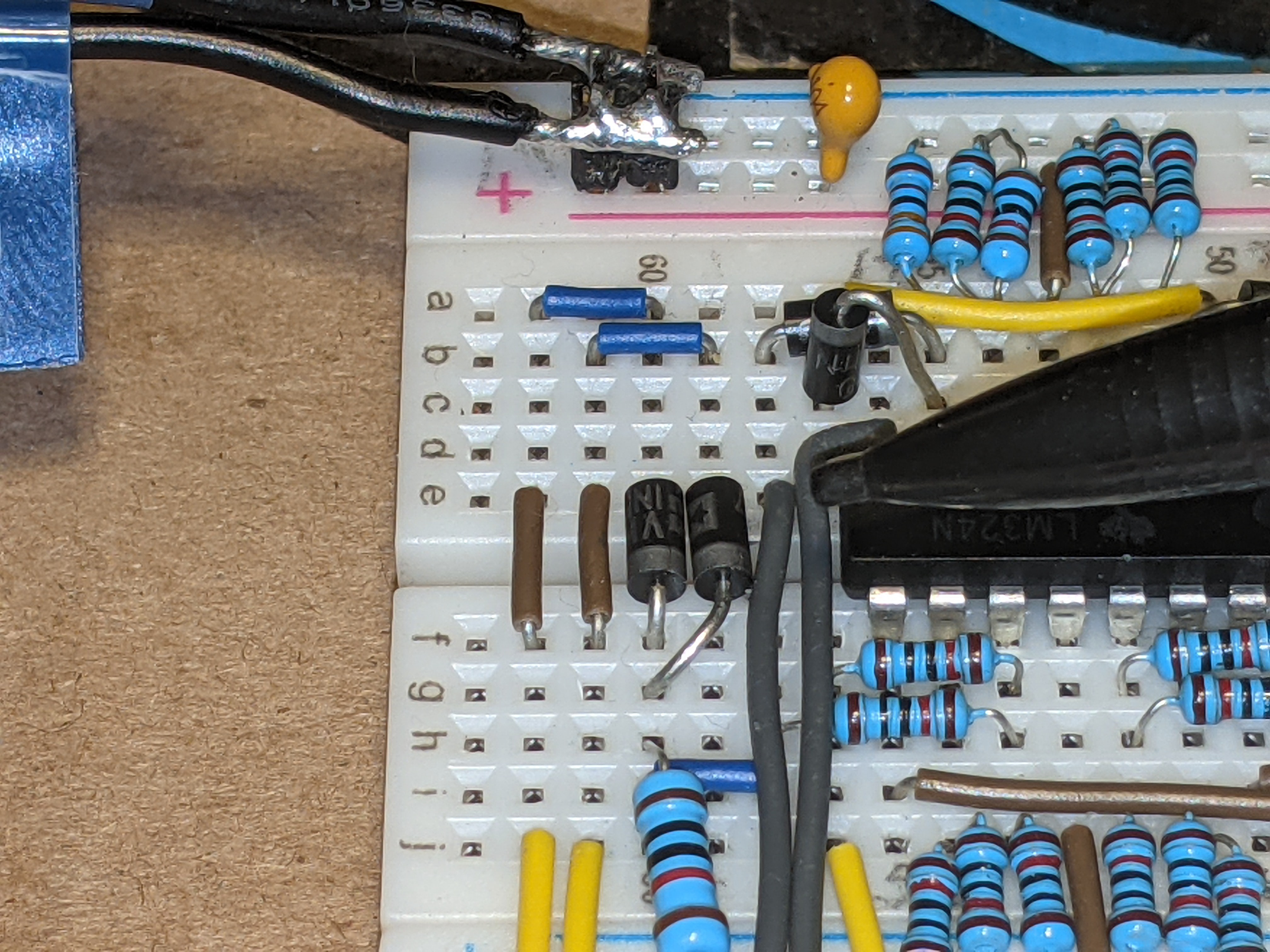
When Built up on a bread board it winds up looking a bit like this:
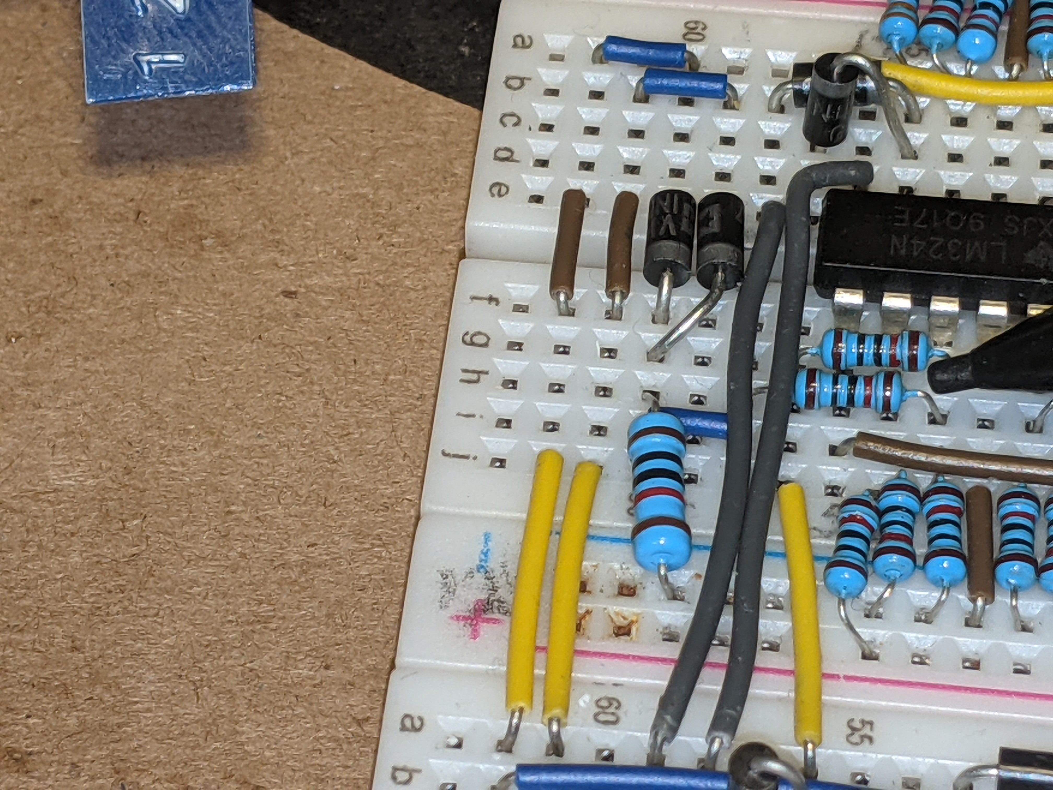
Note the amount of passives required to build up just a single gate; this was a big challenge to lay out on a bread board and make it all work correctly. Each gate requires 2 resistors for a voltage divider on the opposing function input, as well as a grounding resistor and how ever many resistors that are needed to make up the inputs for the gate. If the number of resistors is uneven the resistance values values will be the same, if it is even the grounding resistor on the functional input pin (in the case of a non-inverting circuit this is +) value must be halved:
The reason for this is maths, though, essentially you want the voltage at the divider on the gate input to be greater than ( > ) the voltage on the opposing input leg, to cause the op amp to "rail out" and trigger a high state.
Lastly, to get an inverted function, such as a NAND, You can simply switch the inputs around by placing the divider on the non-inverting pin of the op amp and then using the inverting input for the gate inputs:
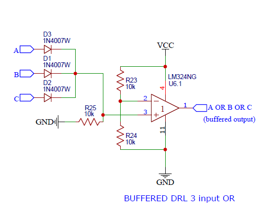
INVERTER / BUFFER / OR
an inverter / buffer is simply just a single input without a resistor and is important for building buffered DRL (diode resistor logic) gates. We need these as using a resistor only set up on the op amp (without using a divider on the input) produces very inconsistent results when chaining in an output from the previous stage of an op amp circuit. This is likely due to the output of the op amp being something less than a high Z state, to make matters worse you can not really assert a low state by pulling the output low with a resistor as it can effect the performance of the next gate.
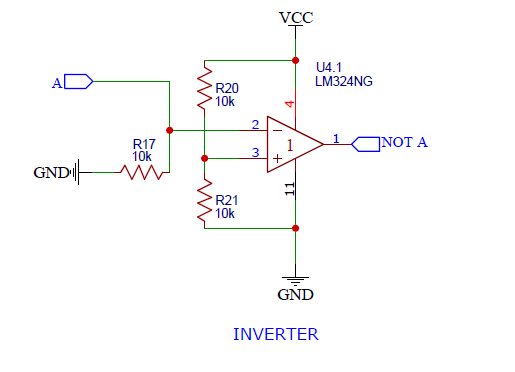
An inverter on it's own is useful enough; but when we build a DRL gate on the input we can produce buffered, inverted output.
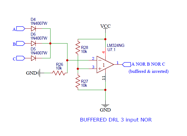
This is the design I went with for my final prototype. I did actually use a resistor or gate on my first build and that worked well because the only or gate that was in the design was on the input of the circuit; and therefore did not have to account for previous stages causing issues with its functional output. When I built the first version of the Z80 1-Bit computational cell I discovered all the issues around that design and had to abandon it. Here is what it looks like built up on the breadboard:
another advantage to DRL is that you can add a or gate to the input of an existing and gate as in the carry stage of the logic diagram without much trouble:
Even if you simply want to buffer the output to bring the overall in line current draw of an output down, by simply building a DRL gate on the input of a non inverting op-amp:
I drew up a simpler schematic for a basic half adder; which shows how gates can be tied together without too much trouble Here:
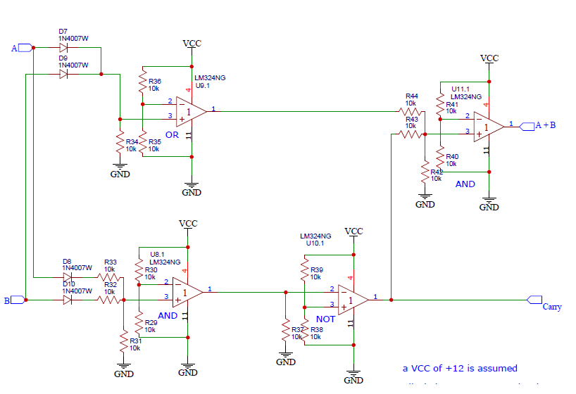
Note D8, and D10: these diodes on the input of the and gate prevent a potential from either one of the inputs from finding it's way to the input of the or gate on top in the case of a half-triggered state. Due to the way that the op amps comparitor works, when wired this way there is a small potential (about 3 volts in this case) that is measured on the non-high pin. Though this is most likely not high enough to trigger the or gate in this case, as you add inputs to your gates this becomes more of a problem and is significantly more difficult to manage. In my opinion building in this protection should be considered best practice for this setup. It's also important to remember current draw of an op amp is higher than traditional logic and you need to be sure to use appropriate tolerance diodes to rule out the higher current from damaging them. Not so much in the case of an AND gate with a large resistor on it's input. But certainly in the case of an OR gate where the output is directly connected to the input of the amp. In all of my test circuit's I used 1A 1N4007 Schottky Power Diodes, this was almost definitely overkill however if you are using switching diodes you may need to pay attention to this condition.
What is next?
As stated before I'd really like to build a state machine based on a 1-bit architecture. Since this thing is really just a large combinational logic circuit; we could accomplish much of this with just a simple eeprom. Using even a 120ns chip we could get speeds that far exceed the MC14500's 1Mhz limit. It would be interesting to see how fast we could get a breadboard computer to run this way using just simple 74 series CMOS chips and a couple of EEPROMS. I'd also like to make a back plane set up and build the whole CPU up on a surface mount card and build the whole thing from the ground up with the possibility for expansion for things like a dumb terminal or a printer. I'd like to perhaps write an assembler and maybe port tiny basic to the CPU as well. Who knows?
You can check out the schematics for the full build in the files section. I also put a bunch of logism files up for playing around with the gates to see how the ALU functions.
Discussions
Become a Hackaday.io Member
Create an account to leave a comment. Already have an account? Log In.