 Mitsuru Yamada
1. Circuit of the SAR ADC
Figure 1 shows the SAR ADC board and Fig. 2 is the schematic.
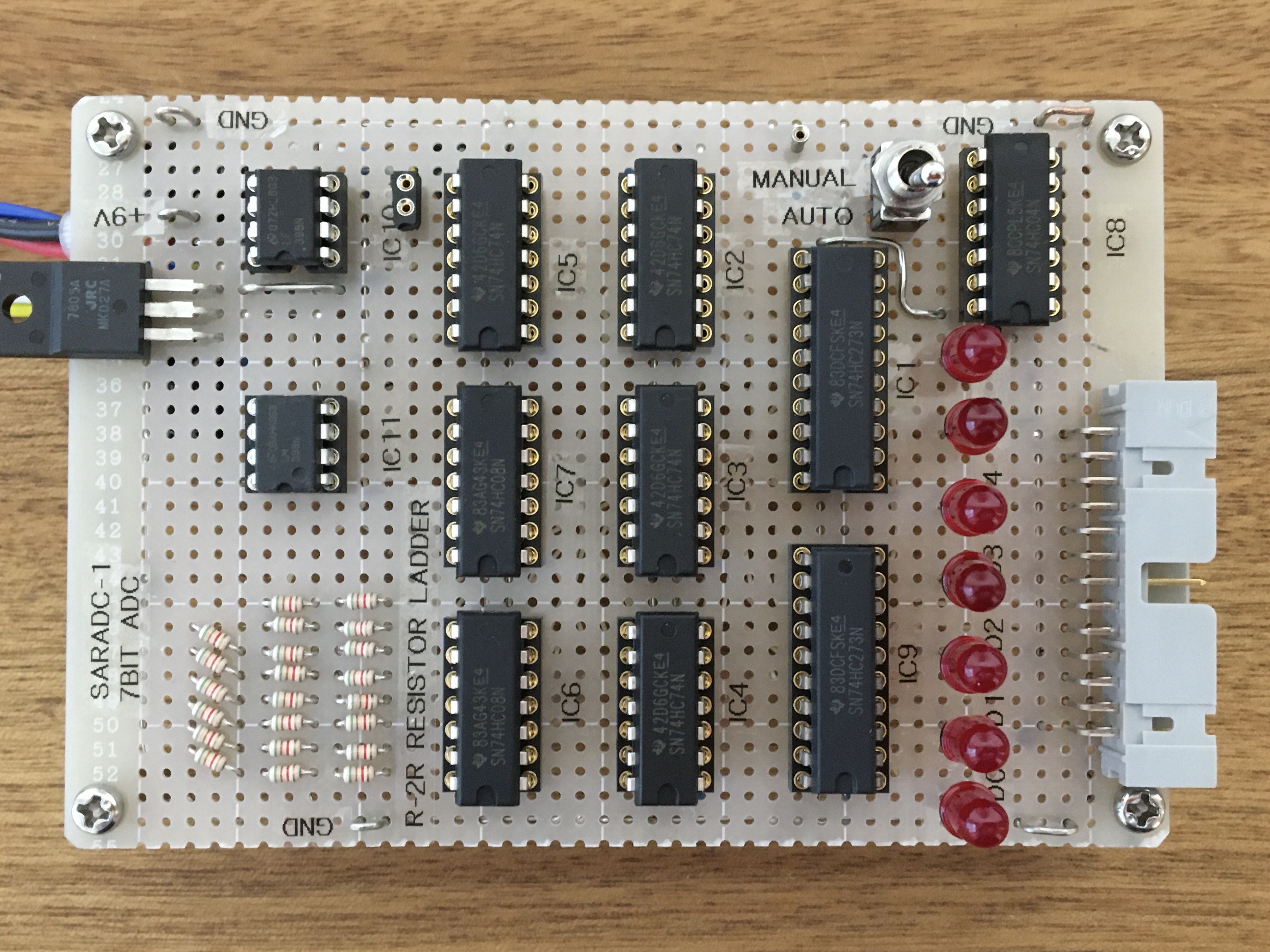
Fig. 1 Circuit board of the SAR ADC
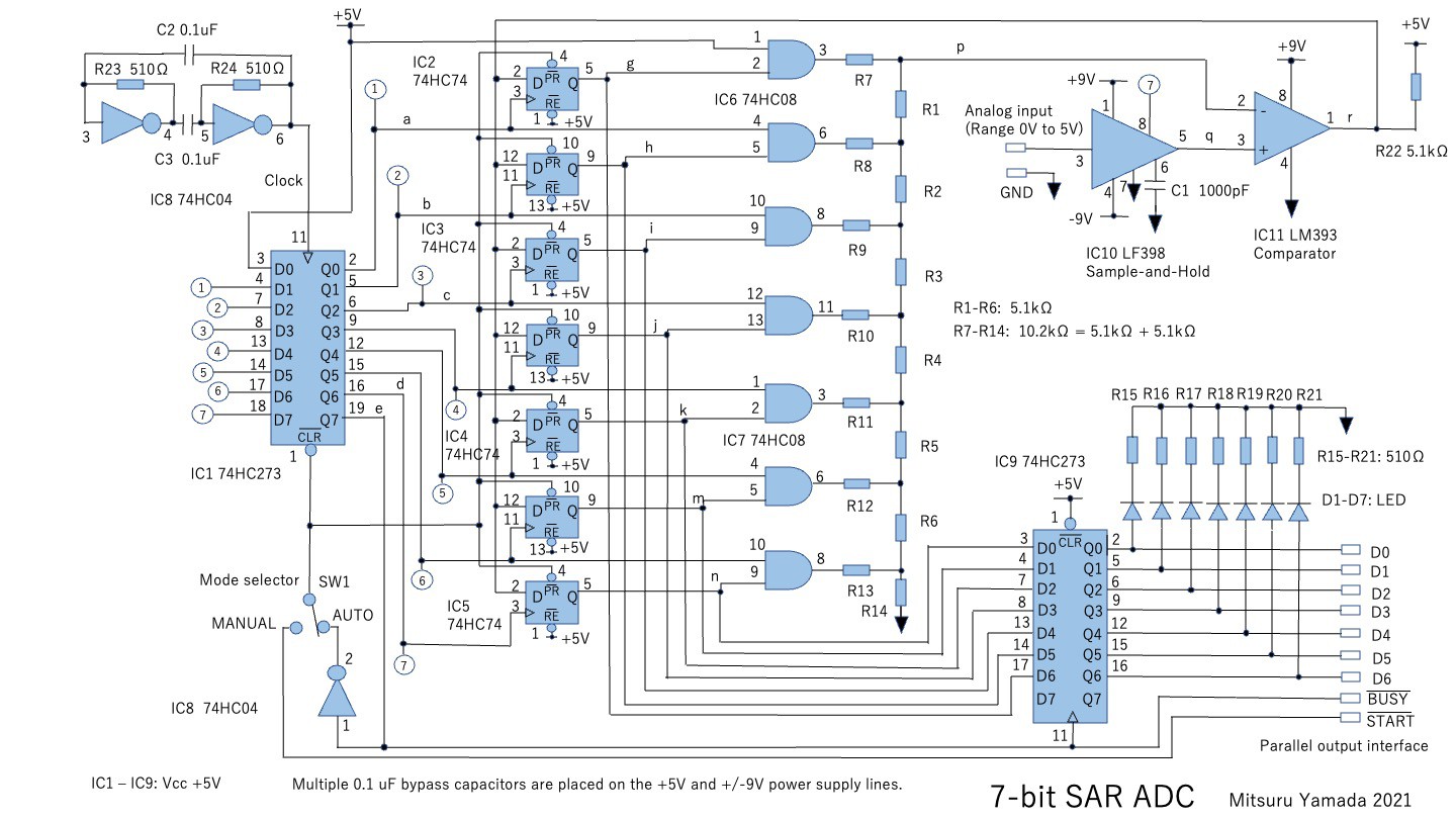
Fig. 2 Schematic of the SAR ADC
The IC1 is an 8-bit shift register. The IC2, 3, 4, and 5 are D-FFs to hold the comparison result of the comparator IC11. The IC6 and IC7 are gates that take the logical product of the shift register output and the D-FF output. The IC9 is a register for holding the AD conversion result. The D1 to D7 are LEDs for displaying the binary data of conversion results. The clock to operate the SAR is generated by an astable multivibrator configured with IC8. The clock period is 103 us and the conversion time is 824 us. The dynamic range of the input signal is from 0 V to 5 V and the output bit width is 7-bit. 0 V is converted to binary '0000000' and 5 V to '1111111'.
2. Internal DAC
The internal Digital to Analog Converter (DAC) that generates the comparison signal with the input signal was configured with R-2R resistor ladder. Normally, it is preferable to use fixed register ladder networks, which have high accuracy, but here, for training purposes, I used individual resistors. The dispersion of the resistors is 1% in actual measurement.
3. Sample-and-Hold
If the input signal changes during conversion, the conversion result will be incorrect, so the ADC needs a sample-and-hold. The sample-and-hold can be composed of an op amp and a FET switch, but here I used a monolithic IC, LF398 [2]. Fig. 3 shows an example of a sine waveform input signal and sample-and-hold output signal displayed on an oscilloscope.
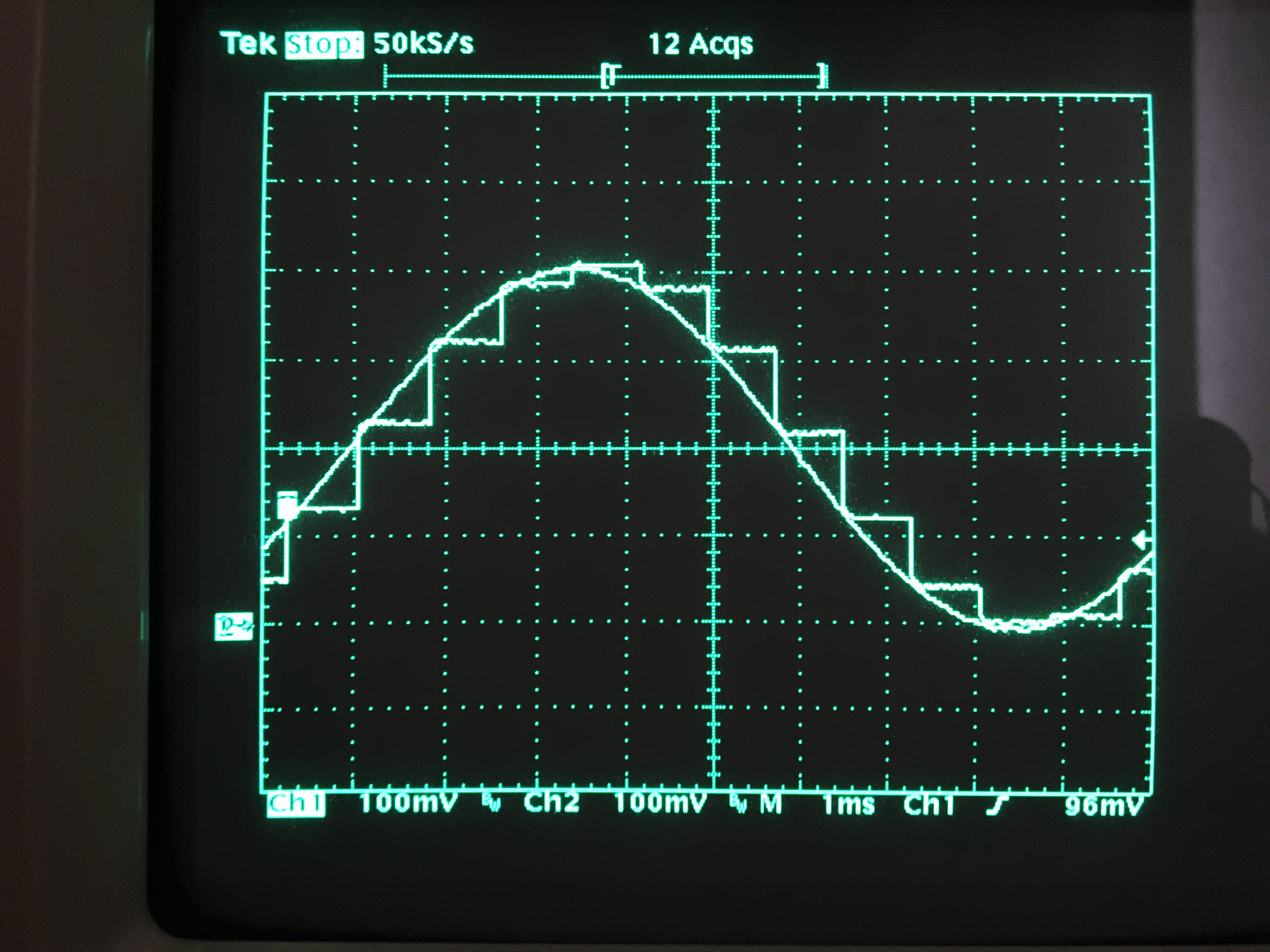
Fig. 3 Sine input signal and sample-and-hold signal.
4. Operation of the SAR
Figure 4 shows the SAR timing. The lowercase symbols in the figure correspond to the symbols of the signals in the schematic in Fig. 2.
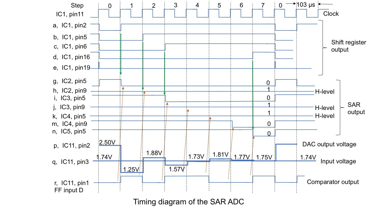
Fig.4 Timing diagram of the SAR ADC
As shown in ‘a’ to ‘d’ of Fig. 4, the shift register of IC1 supplies the rising edge signals, which is shifted by one clock, to the trigger input of D-FFs. This trigger signal causes the D-FF to hold the judgment result of the comparator, as shown in ‘g ‘to ‘n’ in Fig. 4.
In the first step 0 of the SAR operation, all the output bits of the shift register IC1 are cleared to zero, and the output bits of the D-FFs of IC2 to IC5 are all preset to '1'. Each time it move to the next step, the next bit of the shift register is set to ‘1’, and the output of the DAC is add or subtract with a weighting by half of previous, and a judgment is made as to whether it is large or small in relation to the input signal.
The following example shows a case where the input signal is 1.74V. At the beginning of the conversion operation of the step 0, a 2.5V signal, which is half of the dynamic range ('1000000'), is output from the DAC and compared with the input signal by the comparator. Since the comparison signal is larger than the input signal in the step 0, the comparator output 'r' becomes '0'. Then the D-FF output 'g' becomes '0' in the next step 1.
This results in a DAC output of 1.25V ('0100000') in the step 1. Since the comparison signal is smaller than the input signal in this step, the comparator output ‘r’ becomes '1'. Then the D-FF output ‘h’ keeps '1' in the next step 2. This results in a DAC output of 1.88V ('0110000') in the step 2. The output 'i' to 'n' of the D-FF after repeating the same operation is the AD conversion value to be obtained. At begin of next of step 7, this bit pattern is held in IC9 and displaying to LEDs. At this point, the shift register is cleared to zero and returns to step 0.
The actual convergence of the DAC output to the input signal voltage, as observed by an oscilloscope, is shown in Fig. 5. From this waveform, we can also obtain the AD conversion result '0101100' by reading '1' if the DAC output signal increases and '0' if it decreases when transitioning from one step to the next.
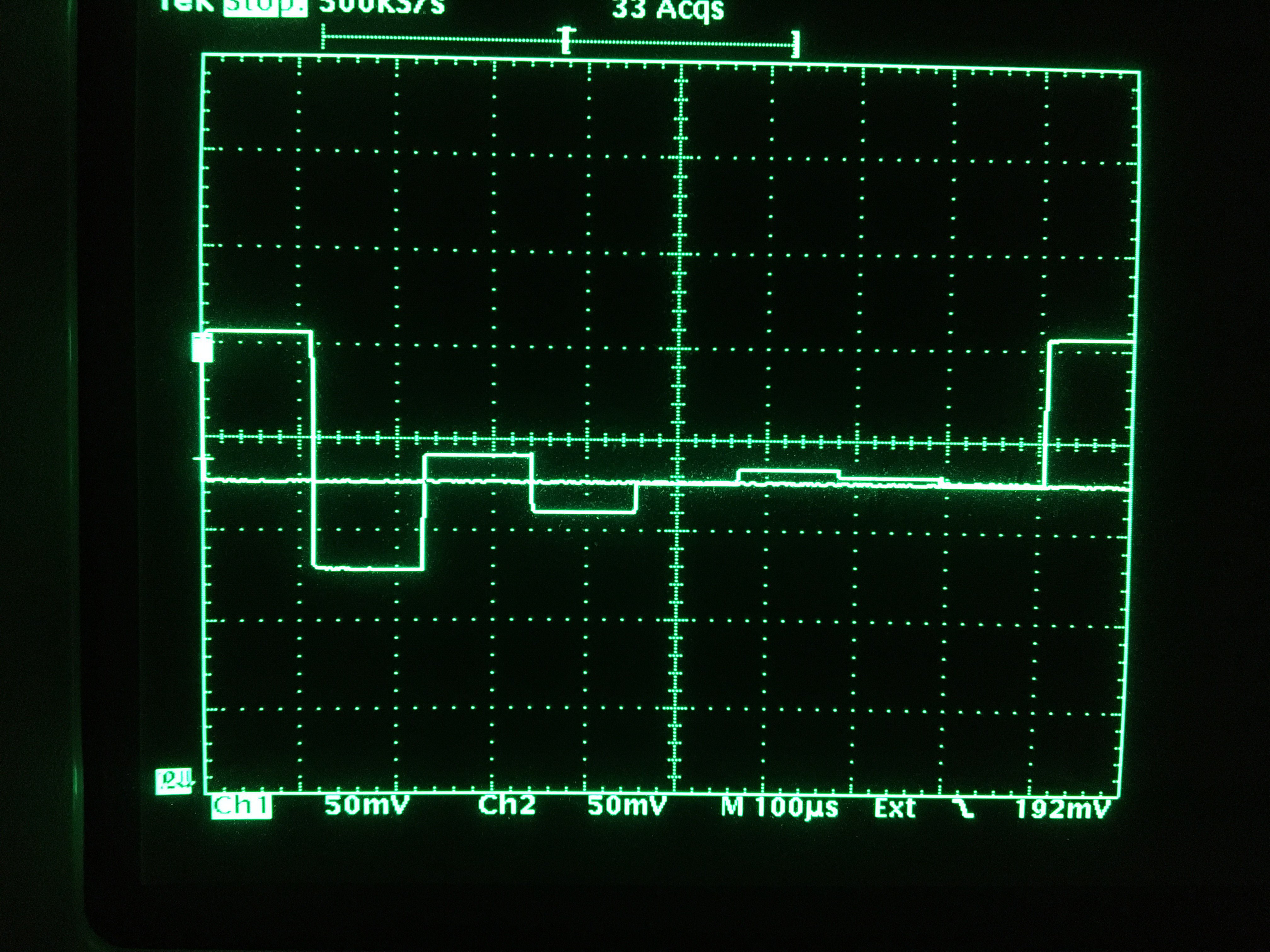
Fig. 5 Input signal (1.74V) and the DAC output signal of the SAR ADC
If you want to add a start signal externally to this ADC instead of using it in self-running mode, set switch SW1 to the manual side. When the start signal transitions from L level to H level, the AD conversion starts. When the conversion is completed, the busy signal transitions from L level to H level, and after confirming this, the external device should read the data from D0 to D6.
5. Video of SAR convergence behavior
In the following Video 1, you can observe the step-by-step convergence of the comparison voltage of the DAC output inside this SAR ADC to the input voltage. There is no audio explanation, so please turn on the subtitle to watch.
Video 1
Video 2 in the following shows an example where the parallel interface of this AD converter is connected to the parallel interface of a computer, and the computer converts the AD conversion values into actual voltages and displays them. Connected is a home-built computer, PERSEUS-9, which accesses the parallel interface with a pointer variable in the CI-2 floating-point interpreter user program to control the start signal and read the busy signal and data. The voltage value displayed is 6 digits, but the correct value is just over 2-significant digits.
Video 2
6. Results
I built a simple SAR ADC using standard logic ICs and observed the convergence behavior of SAR in real time with an oscilloscope for the first time in 42 years. Observing the operation, it is clear that AD conversion with a large number of bits must be considered for noise and linearity. Currently, the ADC is running at 824 us as slow conversion speed, but if the clock frequency and sample-and-hold constants are changed, it should be possible to run up to about 20 us conversion time. I think this SAR ADC is a good example of how important elements of analog and digital circuits can be packed into a small circuit.
7. Appendix
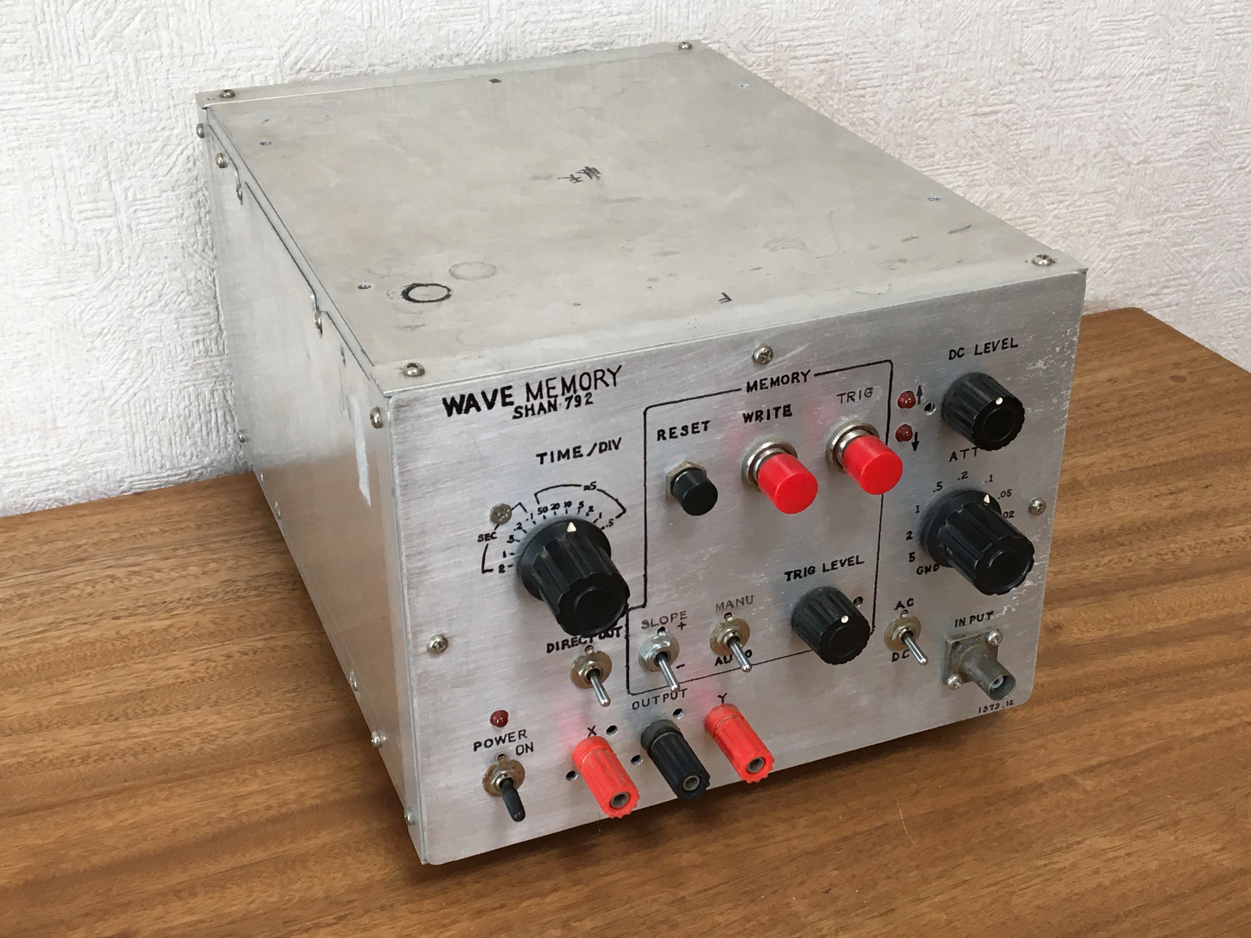
Exterior photo of my own 8-bit digital sampling unit in 1979.
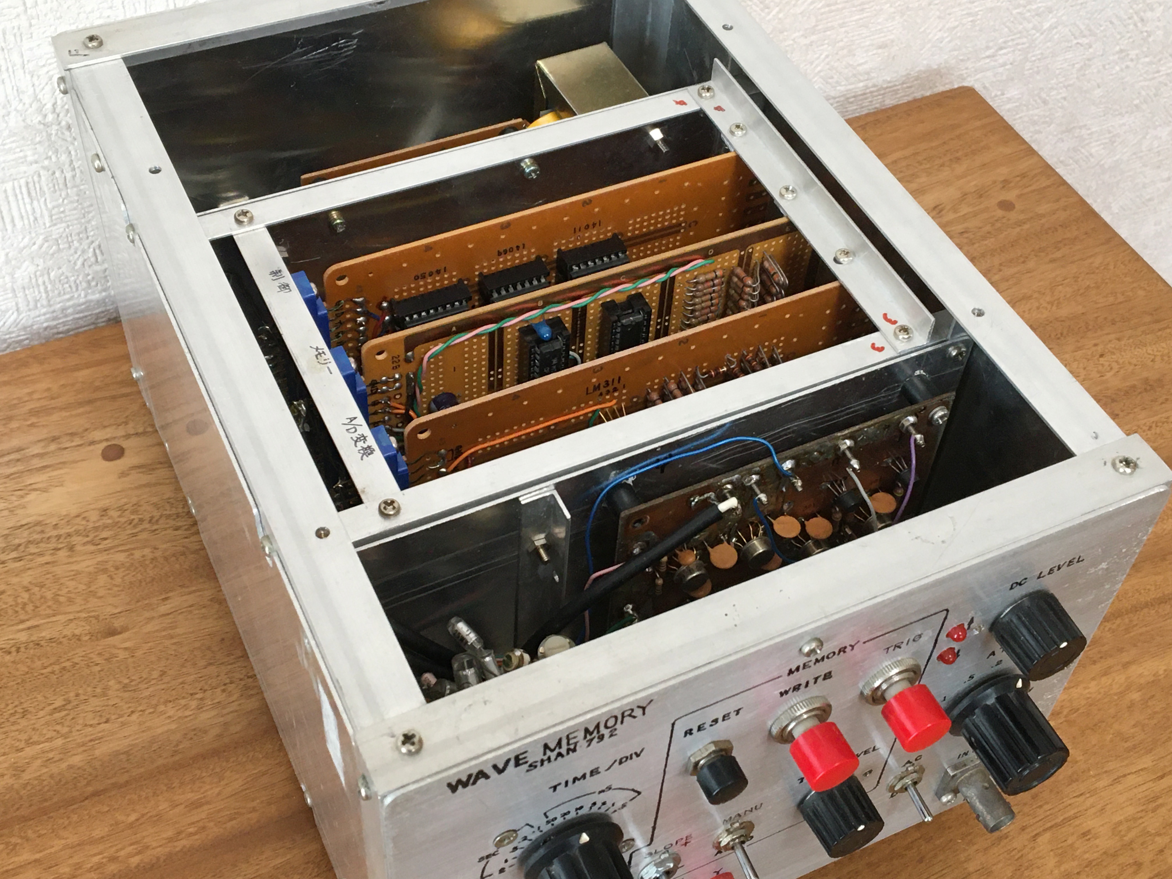
Inside of my own 8-bit digital sampling unit in 1979.
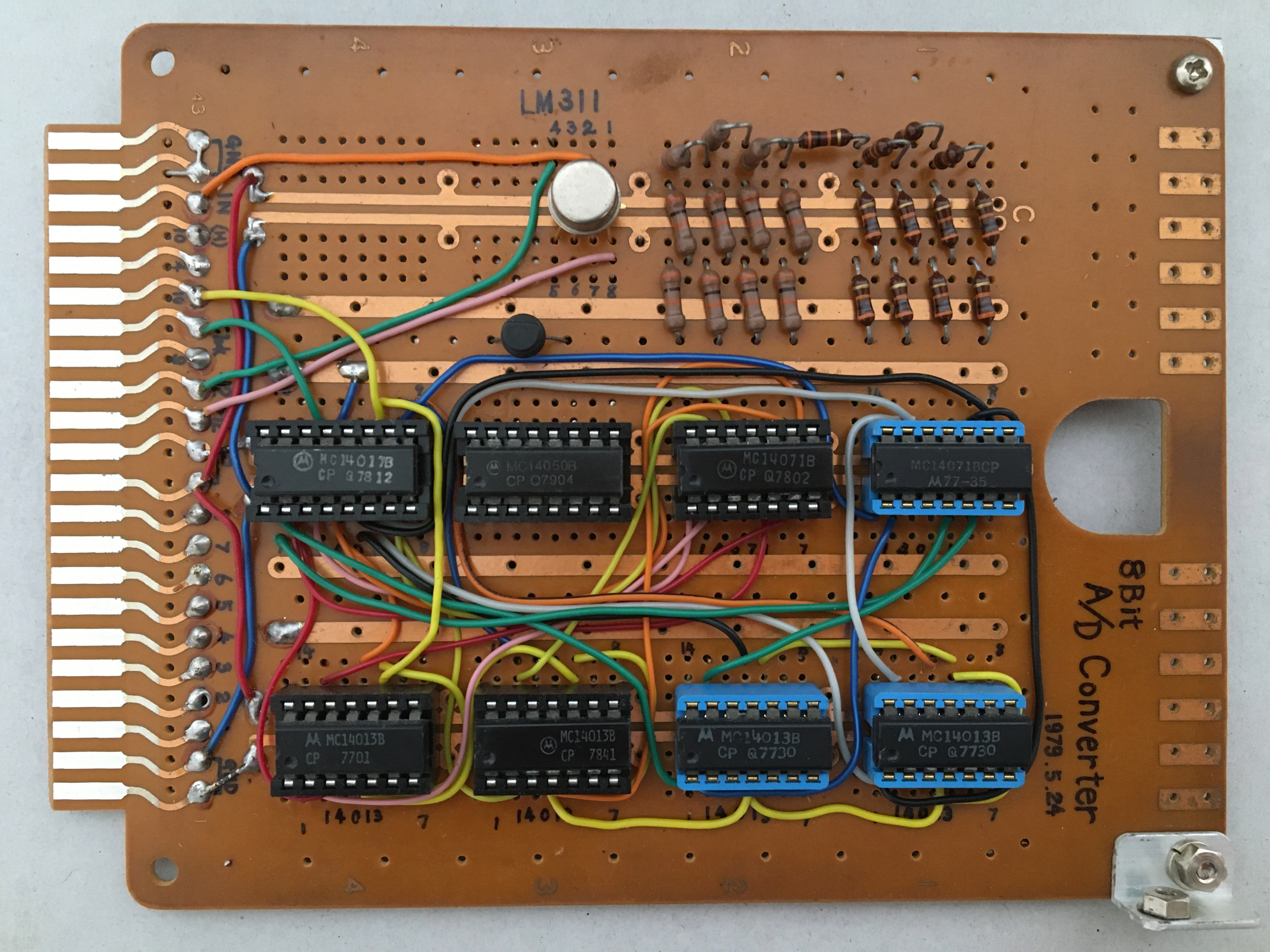
Home-built 8-bit SAR ADC circuit board of the digital sampling unit in 1979.
Schematic of 8-bit digital sampling unit for analog oscilloscopes in 1979.
References
[1] LM393 Dual Comparators, data sheet, TEXAS INSTRUMENTS.
[2] LFx98x Monolithic Sample-and-Hold Circuits, data sheet, TEXAS INSTRUMENTS.
(Posted on Sep. 23, 2021)
(Latest revision on Mar. 31, 2024)