STAR
STARGNSS L1 Signals
The signals in the L1 band produced by the GNSS satellites have a carrier frequency of 1.575 GHz, and contain, among other stuff, the time when the signals were sent and the position of the satellite that send them. Each one of the satellites that send L1 band signals over-writes the information sent with a specific code called de C/A code(Coarse Acquisition).
This technique is called CDMA, and its purpose is to find signals which are below the ambient electromagnetic noise flor. This strategy is also used by other very common communication protocols for example LoRa.
Quadrature Demodulator
Quadrature modulation is a very common and effective technique for modulation data onto high-frequency carriers. Explaining it in detail is out of the scope of the post, but in a very brief summary it amplitude modulates 2 quadrature signals and then combines them for producing any kind of modulation.

Receiver Architecture
Once the downsampled signal is recorded is processed in the ARM and the FPGA by a 4 stage process involving the acquisition, tracking, demodulation, and position computation. This is a very heavy algorithm so the FPGA handles all the DSP stuff while the ARM sticks altogether and builds the NMEA message which then will be sent by SPI to the flight controller.
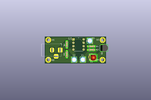
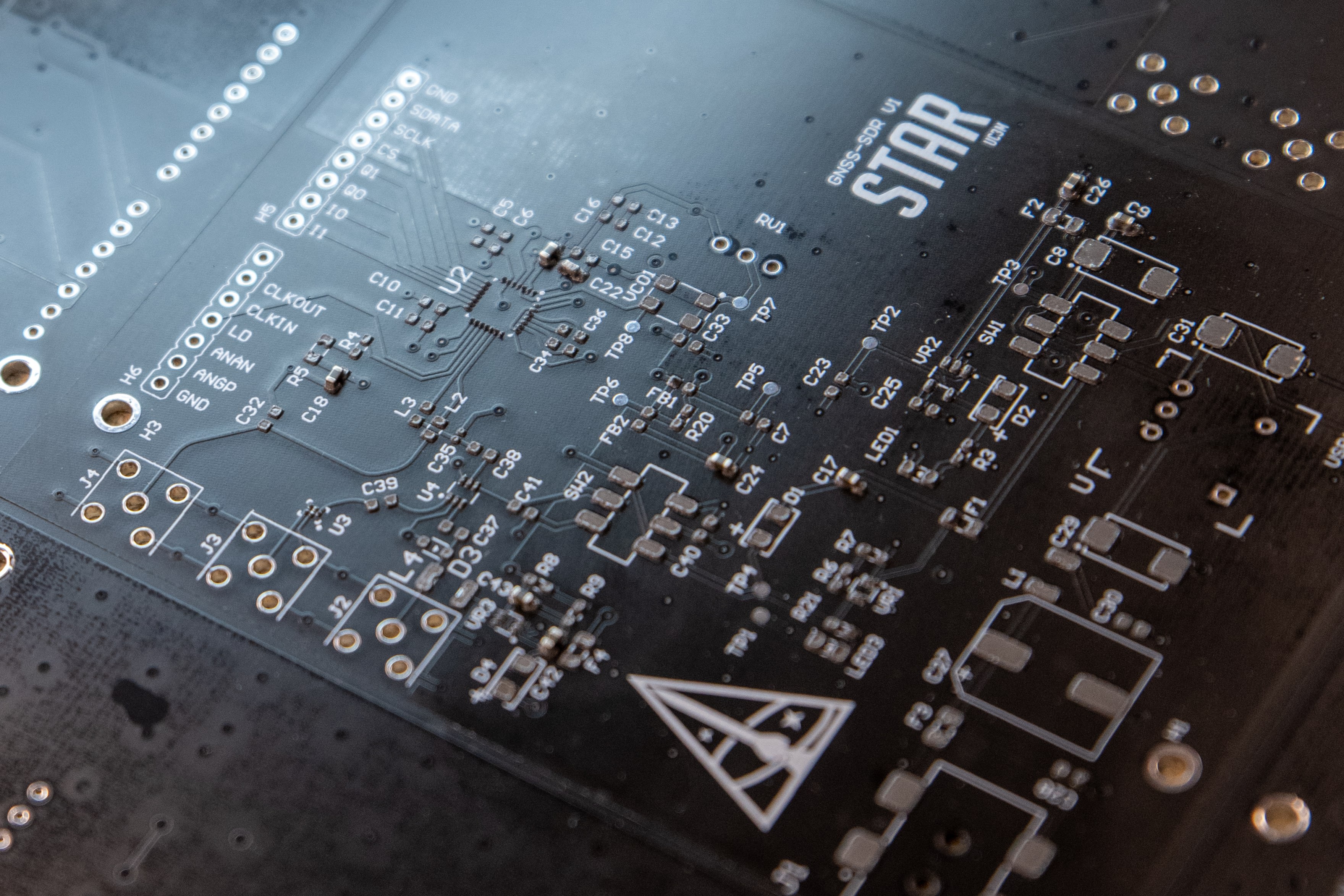
PCB Manufacturing
For the schematic and the PCB design, we have used Altium Designer, a great software with tools for impedance control and high-frequency signal integrity. The manufacturing of the boards was done by our sponsor JLC PCB and they have lived up to the expectations with very nice finishes and perfect impedance controlled traces.
All the board has SMT parts and has been soldered with a stencil provided by JLC PCB and the soldering process took place on the Carlos III University
Ordering the PCBs at jlcpcb
This project is sponsored by jlcpcb. jlcpcb is a full feature Printed Circuit Board manufacturing service.
Turn your DIY breadboard circuits into professional PCBs – get 10 boards for approximately $5 + shipping (which will vary depending on your country).
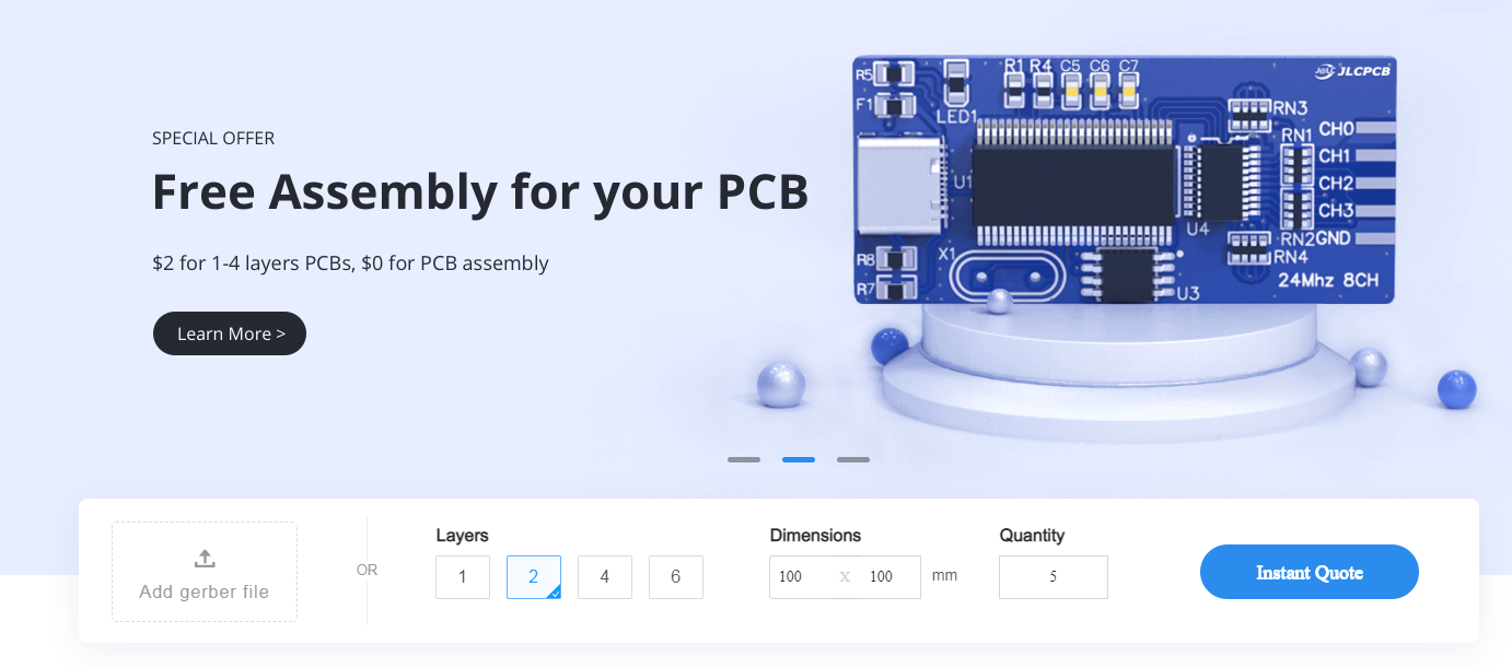
Once you have your Gerber files, you can order the PCB. Follow the next steps.
1. Download the Gerber files – click here to download the .zip file
2. Go to jlcpcb website and Click on Quote Now button.
3. Upload the gerber file you downloaded in the last step. Upload the.zip file or you can also drag and drop the gerber files.
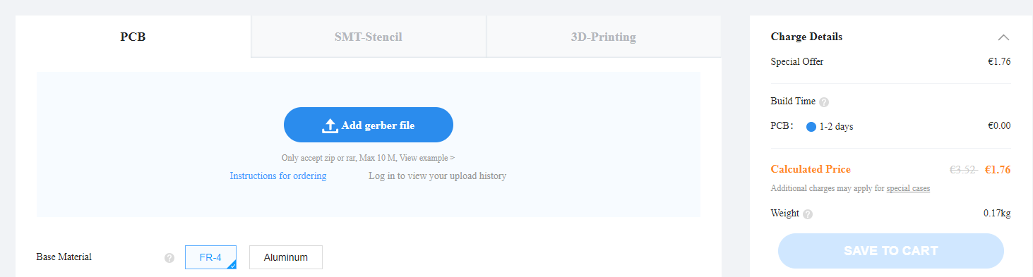
After uploading the zip file, you’ll see a success message at the bottom if the file is successfully uploaded. You can review the PCB in the Gerber viewer to make sure everything is good.
jlcpcb can grab all the PCB details and automatically fills them for you. But you can also
To place the order, click on “SAVE TO CART” button
Before finalizing your order you can use the promotional code JLC-REBE to get a discount and then click pay.
 mbsg99
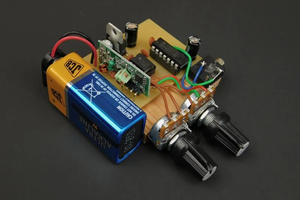
 Mrinnovative
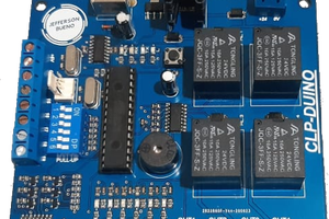
 Jefferson Bueno