 kelvinA
The component
I want to see ASAP if I'm out of pins. I was going to just line up some pins someplace in the schematic to show "this is where a pad goes, but I don't know the fine details of it just yet". However, I was stuck like a frozen loading bar and decided (after taking a little browse to see what my other ECAD options were) to just make an actual component for the thing:
The cool thing is that there are 2 open source PCB schematic designs for this screen, from waveshare and dfrobot.
Back to talking about Fusion 360, I found out a couple things. First, I can change the theme in Preferences, and I changed the PCB/footprint editor to light (because I first changed the schematic editor to dark and it was harder to see), and the second thing I did was change the default grid to mm (since I'm mostly coming across mm specified pin layouts or it'll be something classic like 2.54mm anyway).
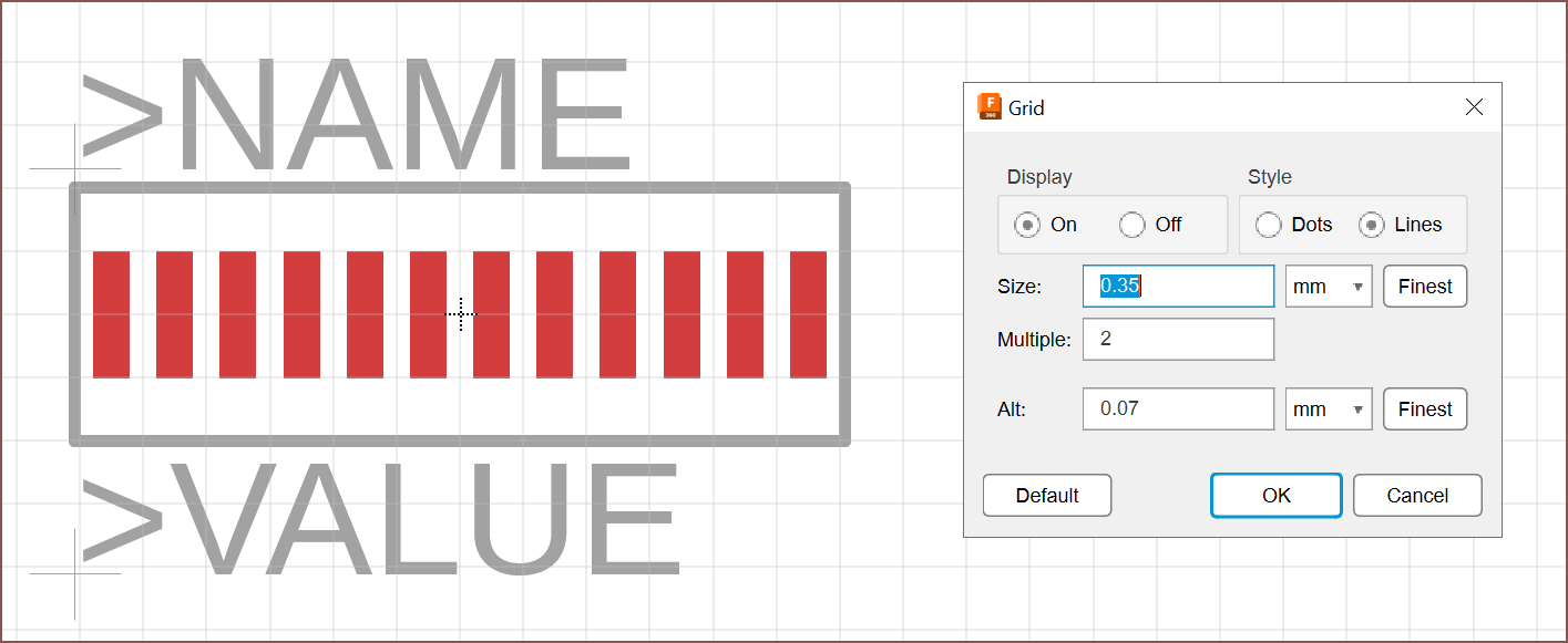
For this LCD, the spacing is 0.7mm as claimed on the listing. Now, I thought I could just use the pin array and have my alts set to 0.35mm, but for some reason, after I click to place the pad, it nudges over to the nearest 0.7mm (which was my grid size when I tried it). Thus, I've come up with this better strategy which is to have half the grid size with "Multiple" set to 2.
Thankfully, this now means that creating this pad (and others similar to it) is super easy, barely an inconvinience, meaning that I don't have to worry too much about perfection straight out of the gate. I've used 1.4mm * 0.4mm pads currently, but this might increase to 2mm if the pads still seem like they'd be harder to solder.
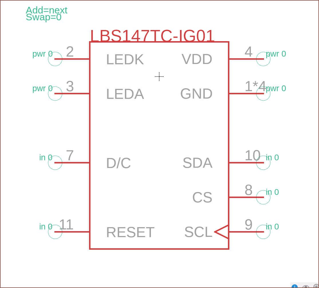
Back to talking about the symbol, I've decided to keep things consistent with other components instead of doing the more traditional thing of listing out all 12 pins. Still, I haven't done any consistency tweaks like swapping LEDA and K around so that the +ve of the LEDs (LEDA) is inline with +ve of the pad itself (VDD). I'm also wondering if I should stay consistent and have the symbol be 12 squares wide instead of the 8 it currently is.
The circuit
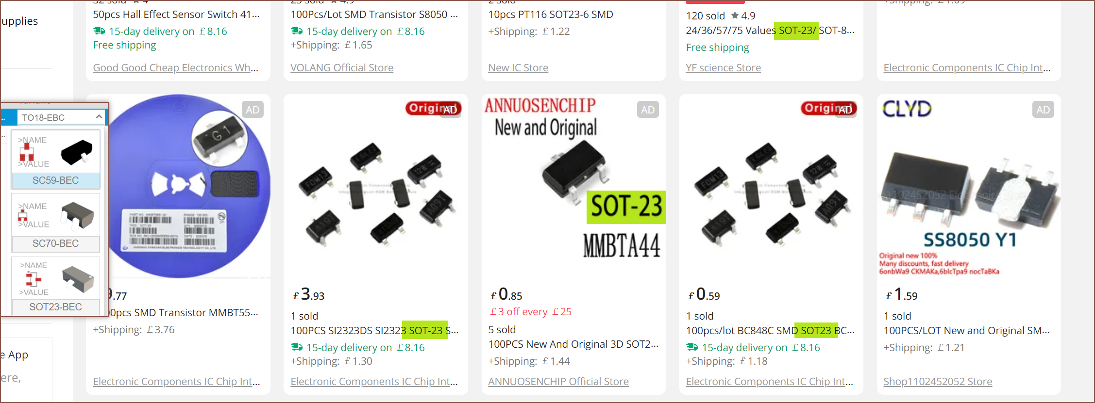
The backlight circuits in both PCB designs call for some NPN transistor. I looked at my options already available in Fusion360 and then searched "npn smd" in AliExpress. It seems that the SOT23 is the most common:
After that, it seems like it's just a quick slap together of components and pin names to get... this run:
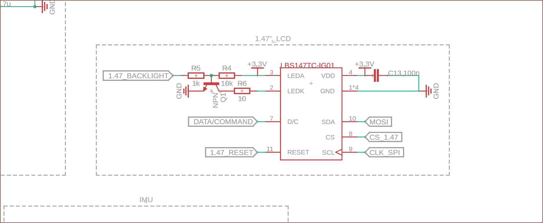
This means that I'm another 4 pins down, and I haven't even looked into I2S yet. I doubt I could just send audio down through I2C so I better look into that next.
Discussions
Become a Hackaday.io Member
Create an account to leave a comment. Already have an account? Log In.