 Phil Wright
Thanks to Yann Guidon for pointing out how the design of the register file could be improved in order to save on components. In fact the previous design used a total of 255 IC's over 45 PCB's. Based on the feedback I have come up with another design that brings the number down to 138 IC's and 18 PCB's. Quite the saving!
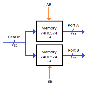
The Register Store design has been changed to remove the use of separate output buffers and instead uses the built in output buffering capability of the 74HC574 IC. In order to make that work we need to store the value twice, once per output port and then use an incoming enable line in order to control when the value is output. Although crowded, we can fit the 8 x 74HC574 and all the headers onto a single board and so reduce the number of PCB's by half as well as saving on IC's. The block diagram is very simple...
We used to have a Register Select for each register. But instead of providing the register numbers to each register we can use a de-multiplexer to convert the binary numbers into selection control lines that are then distributed to each storage board. That means we have the selection logic once rather than for every register. Here is the block diagram for dealing with the register write functionality...
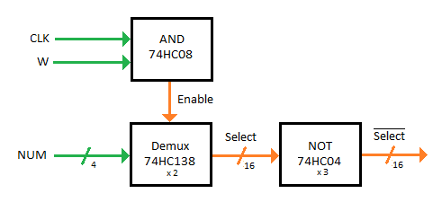
The NUM is just a 4 bit binary number that comes from the instruction and is the target register to be written to. But we only want to write when the CLK occurs and the W (write) control line is high. Instruction decode logic elsewhere will decide if the W should be high based on the specific needs of the instruction. We need 2 x 74HC138 IC's to perform the de-multiplexing resulting in 16 output select lines. Because the 74HC574 memory IC needs an active low signal for writing a new value we need to invert all 16 lines before distribution.
Two more copies of this board are needed in order to generate the port A and port B output signals based on values from other parts of the current instruction. They are simpler in that they do not care about the CLK and W signals, they always output something on both ports at all times. To keep costs down I will use the same design for all three boards but the port A and B instances will have jumpers that connect the CLK and W to high so that the output is always applied.
I should be able to get this designed in Eagle during the next couple of days and then ordered.
Discussions
Become a Hackaday.io Member
Create an account to leave a comment. Already have an account? Log In.
Hi! Cool project!
I can't understand how you register file works. The RISC-V architecture uses up to three registers in command: two operand registers and one destination register (e.g. ADD x1, x2, x3: x1 = x2+x3). I understood the hack with operands, but writing still no clear. You register file has two address inputs "AE" and "BE" for selecting register for bus "A" and "B". But how you select the register for "Rd" (destination)? According you desing data from "Data In" bus will be write to the register selected by "NUM" on "CLK & W" signals. You should write to both register files simultaneously. So you need perform read operation by passing "rs1" and "rs2" for AE and BE, than perform write operation by passing "rd" both for "AE" and "BE" and setting high W. So, you should store ALU result somehow. You use additional trigger for ALU result?
Are you sure? yes | no
I will not be pipelined, one instruction per cycle with no pipelining. The complexity of the control and data hazards is for a future project maybe!
Are you sure? yes | no
one instruction per cycle is already great :-)
Are you sure? yes | no
Oh! Two address spaces makes more sense now.
Are you sure? yes | no
More optimisations to come :-) I hope you haven't already ordered PCBs ;-)
* The 138 has "inverted" outputs so you shouldn't need the inverters.
* In case you actually needed inversion, simply use the 74HC238 which has "positive active" outputs
* use the provided auxiliary enable inputs of the 138/238 as much as possible :-)
* If all you need is 16 low-active outputs, the 74HC154 does it in one single, larger DIP chip.
I might sound picky but actually I am eager to see this thing work soon so I push you a little and point at the problems and their solutions because you face them :-)
PS: it's not "homebew" but "homebrew" ;-)
Are you sure? yes | no
Thanks again for the feedback. Guess I misread the spec and did not realise the outputs were inverted already. Using the larger 154 I might be able to cram everything on a single board instead of across 3. I will investigate that when I get home tonight. Yes I did already order 5 different types of PCB, but only one needs to be redone and that is only $10. So no big deal. Although I might end up with quite the collection of failures at this rate.
Are you sure? yes | no
you can still make art stuff with them :-)
Are you sure? yes | no
Oh and there might not be a need to respin the decoder boards. Just wire/short the input to outputs and don't populate the inverter chips :-)
Are you sure? yes | no
You could, at the cost of a few clock cycles per instruction, reduce your part count further by not implementing a dual port register unit. Put two latches at the inputs of your ALU and then load the values in serially. In saying that I'm picturing a dumb microcoded design. What sort of control unit are you envisioning?
Are you sure? yes | no
obviously he's doing a RISC-V so microcoding it would add more issues than "solve" or "save" anything... The register set is usually under-valued but look at the ARM-1 : it takes half of the die area.
A good register file is half of the work to design a good CPU :-)
Are you sure? yes | no
There will always be a certain amount of complexity involved, the design process is where you figure out where it all ends up. He could lobotomize the design (from a philosophical standpoint: tainting a RISC design with microcode) and cheat in a few areas (an EEPROM for microcode and a few old GAL/PAL chips for decoding).
Building a CPU on perfboard makes that line of thinking more palatable (fewer wires to solder, but a slower, "dumb" design), but since he's buying boards the question was if he is doing everything the "right" (RISC) way or not.
Are you sure? yes | no
I want to avoid using microcode in order to get better performance . Not sure why but I kind of feel that using microcode is cheating. My first design will be a single cycle design with separate instruction and data memory banks so I can load an instruction and write or read from data in the same cycle. Once I get to the point that the CPU actually fully works and is debugged I might be tempted to have a single combined instruction/data bus and sacrifice some performance because data instructions then take two cycles instead of one. But that kind of decision is a long way off yet.
Are you sure? yes | no
I wouldn't go so far as to call it cheating, but it certainly wouldn't be how a RISC design is traditionally implemented.
Going for a single cycle design actually makes your project more interesting. I've never done a pipelined processor so I can't wait to see where you end up with things.
Are you sure? yes | no