 ElectroBoy
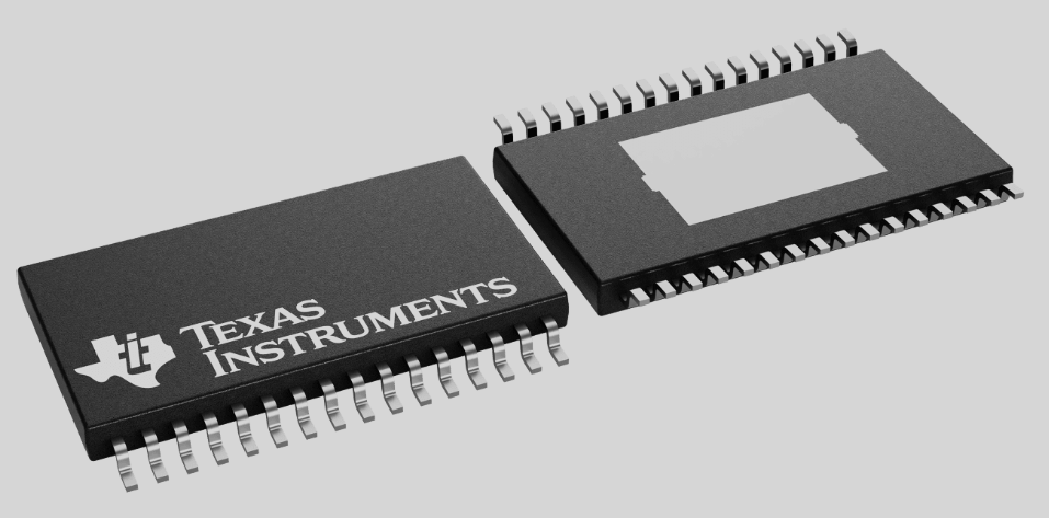
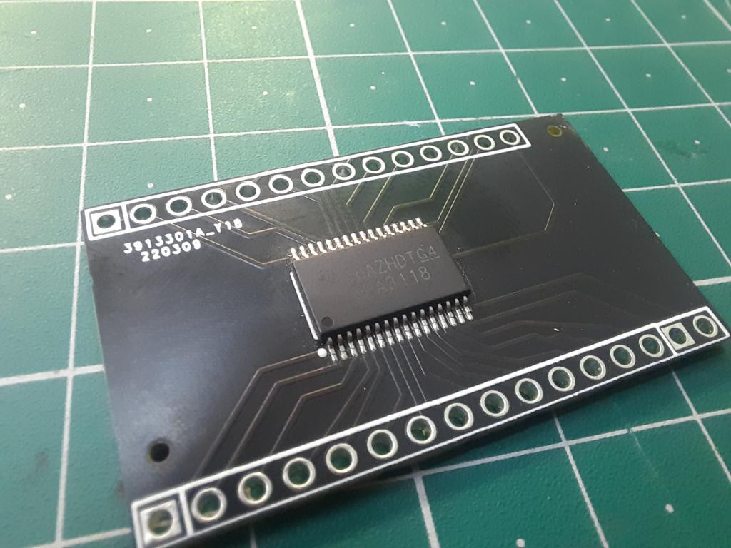
I am here with my own Class D amplifier as promised in the last articles. Because Class D amplifiers are used in audio equipment’s on large scale. So, I tried to design myself to understand the working principle and classification of integrated circuits used in Class D. As mentioned in previous article I am using breadboard compatible IC shield to try different components. I have TPA3118 series IC which can output a maximum of 60watt in bridge mode. You can also use this in stereo mode to output 30 watts per channel. Here I am sharing the datasheet with you.
TPA3118D2 and family:
The TPA31xxD2 series are stereo efficient, digital amplifier power stage for driving speakers up to 100 W / 2 Ω in mono. The high efficiency of the TPA3130D2 allows it to do 2 × 15 W without external heat sink on a single layer PCB. The TPA3118D2 can even run 2 × 30 W / 8 Ω without heat sink on a dual layer PCB. If even higher power is needed the TPA3116D2 does 2 × 50 W / 4 Ω with a small heat-sink attached to its top side Power PAD. All three devices share the same footprint enabling a single PCB to be used across different power levels.
Features
- 2 × 30W Into an 8-Ω BTL Load at 24 V (TPA3118D2)
- Wide Voltage Range: 4.5 V to 26 V
- Efficient Class-D Operation
- Programmable Power Limit
- Differential and Single-Ended Inputs
- Stereo and Mono Mode With Single-Filter Mono Configuration
- Single Power Supply Reduces Component Count
- Integrated Self-Protection Circuits Including Overvoltage, Undervoltage, Overtemperature, DC-Detect, and Short Circuit With Error Reporting
- –40°C to 85°C Ambient Temperature Range
Components required:
1) 100K and 20K resistors
2) 1uf, 220nf, 100nf, 10nf, 1nf ceramic or polyester film capacitors
3) 1000uf, 47uf electrolytic capacitor
4) 100uh-330uh inductor coils
5) 24volt SMPS @5amp
6) 50-100watt speakers
8) Preamplifier (Optional)
Circuit used:
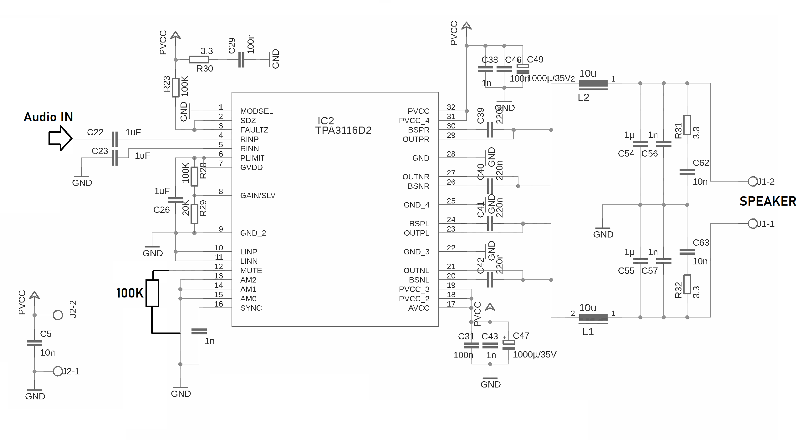
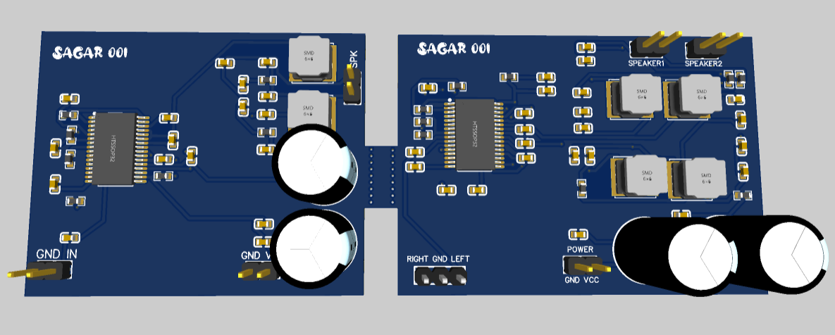
After trying a lot of circuits and checking the sound quality, noise, pop sound and amplifier response curve for gain. I designed this schematic in EasyEDA. Because this IC can work in both stereo and mono channel so I designed two compatible circuits.
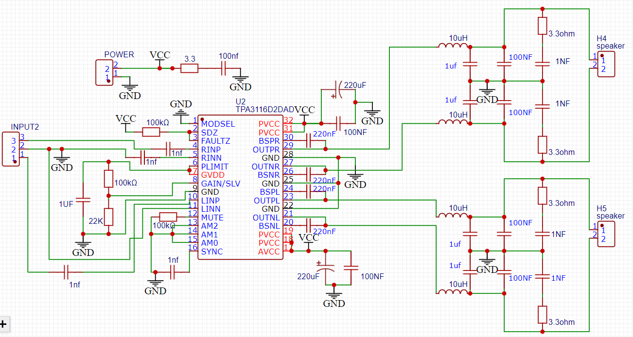
Which can be then modified into PCB (2 designs on a single board, which reduce the cost of assembly and overall PCB. I always use JLCPCB for my projects because they are providing standard PCB assembly, manufacturing and much more in very low price. Sign-up using this link and get $54 new user coupons. Checkout to JLCPCB right now and try best experience of PCBA.
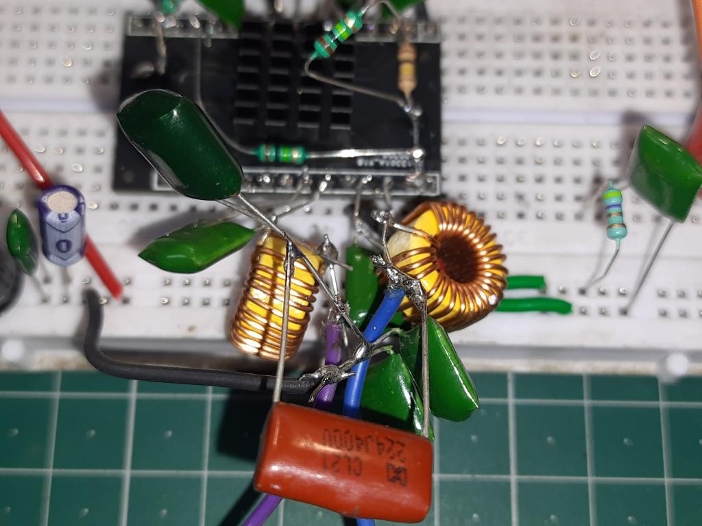
Breadboard Circuit:
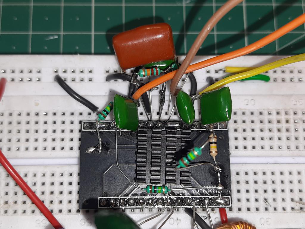
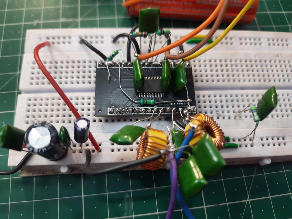
Breadboard schematics is designed as per circuit diagram shown above. I am using only 1 channel with a max output of 30watts. Which is used to drive one speaker only. All the circuitry is supplied with 12v @2amps.
Coil (L-C filter setup):
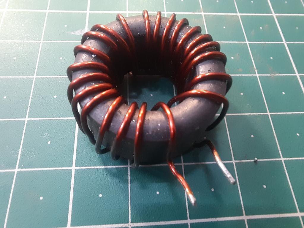
In the circuit 10uh is the recommended value of the inductor. But we can use 100uh to 330uh inductor in combination with a 220nf to 1uf capacitor for a better frequency response from the LC filter. This will reduce the overall noise and give a stable signal to speaker to tune accordingly with low, mid and high frequencies.
Heatsink assembly:
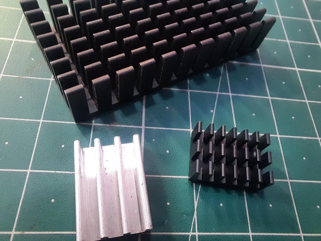
Because we are testing this amplifier in raw conditions with variable power supply unit and gain resistors. A heatsink is mandatory for that, IC may be generated heat in low load resistance conditions. This 3118d2 can output a maximum of 60watts or 30watt per channel without heatsink.
Power supply:
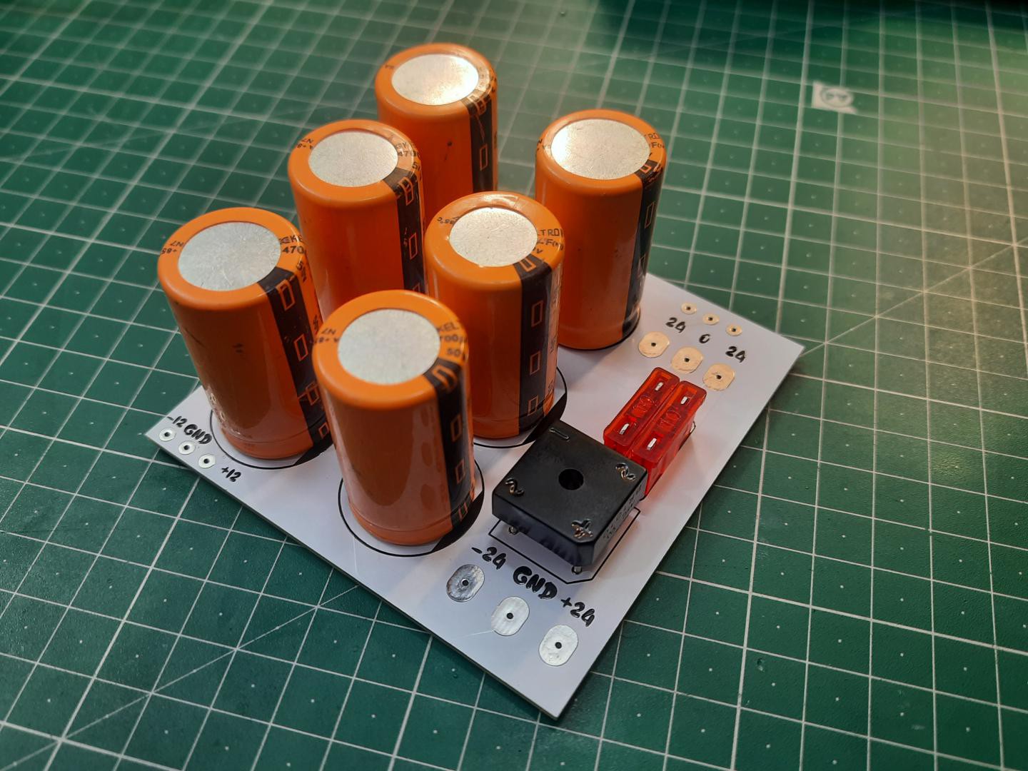
The working of class D amplifiers are discussed in previous article you can see that from here. Because we are using LC filter to reduce the square PWM into audible signal. That’s why a filtered power supply is recommended with these class D amplifiers. Either we can use a SMPS or High filtered DC supply for power input.
JLCPCB Assembled PCB:
At my place here in INDIA, Class D integrated circuits are not sold separately. If I want to play with Class d then I have to buy a full amplifier system. Which will cost me more and out of the interested area. That’s why I planned to go with PCBA service of JLCPCB. Previously I designed this breadboard compatible shield on which I am testing this amplifier.
Working:
I mounted everything on a small piece of breadboard. And after testing for an hour, I found- At higher volumes amplifier is turning off with a pop sound. This is because of power limit and gain resistor setup. I don’t have ceramic capacitors of recommended values so I used polyester film low value capacitors.
If you are using this amplifier in stereo channel then same value resistors, capacitors and inductors are required on the output stage. Inductor coils matters a lot in this circuit, higher the value greater will be the frequency response.
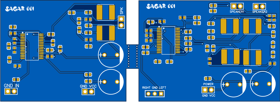
Then I designed the PCB according to the schematics given above. I combined 2 designs in one and order it from JLCPCB SMT assembly service. I will share the Gerber files, BOM and CPL soon once after testing these layouts. Till then stay tuned, follow us on Hackster, hackaday and instructables.