 Dave Collins
Here we go.....
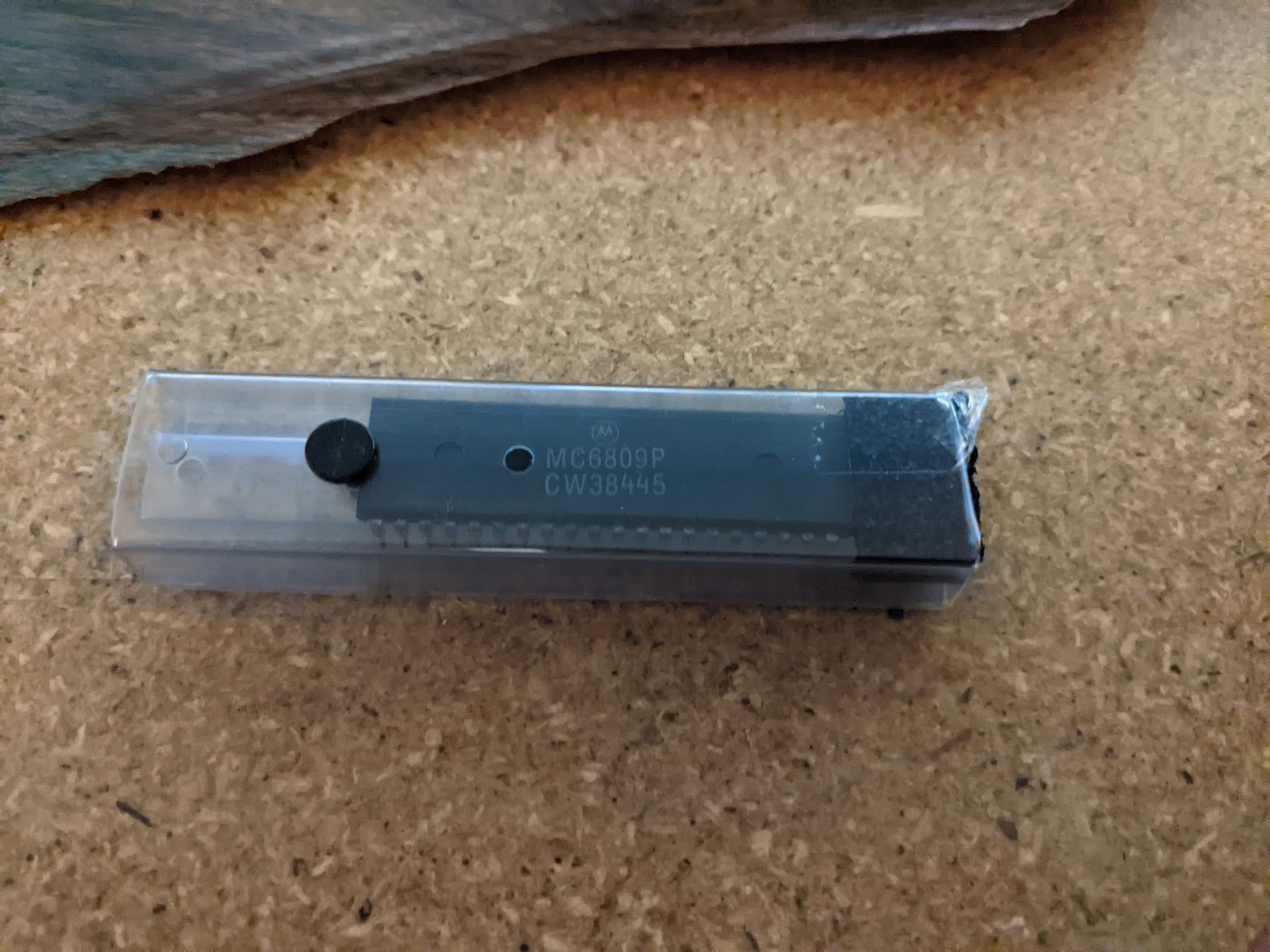
So I needed a pallet cleanse of my CMOS CPU project that's kind of hit a snag. I bought this 6809 in a vintage electronics suppler that is about 40 minutes from my house called Chester electric. They are a small electronics suppler and they have everything! Seriously from HAM parts to boards you can buy to pull micro's off of; it is my happy place. I never manage to take pictures when I'm there but here is a video Rinoa's Auspicious Travels took of the inside of the place:
if you are ever in southeast Wisconsin its a very interesting place to visit, I highly recommend it!
The CPU:
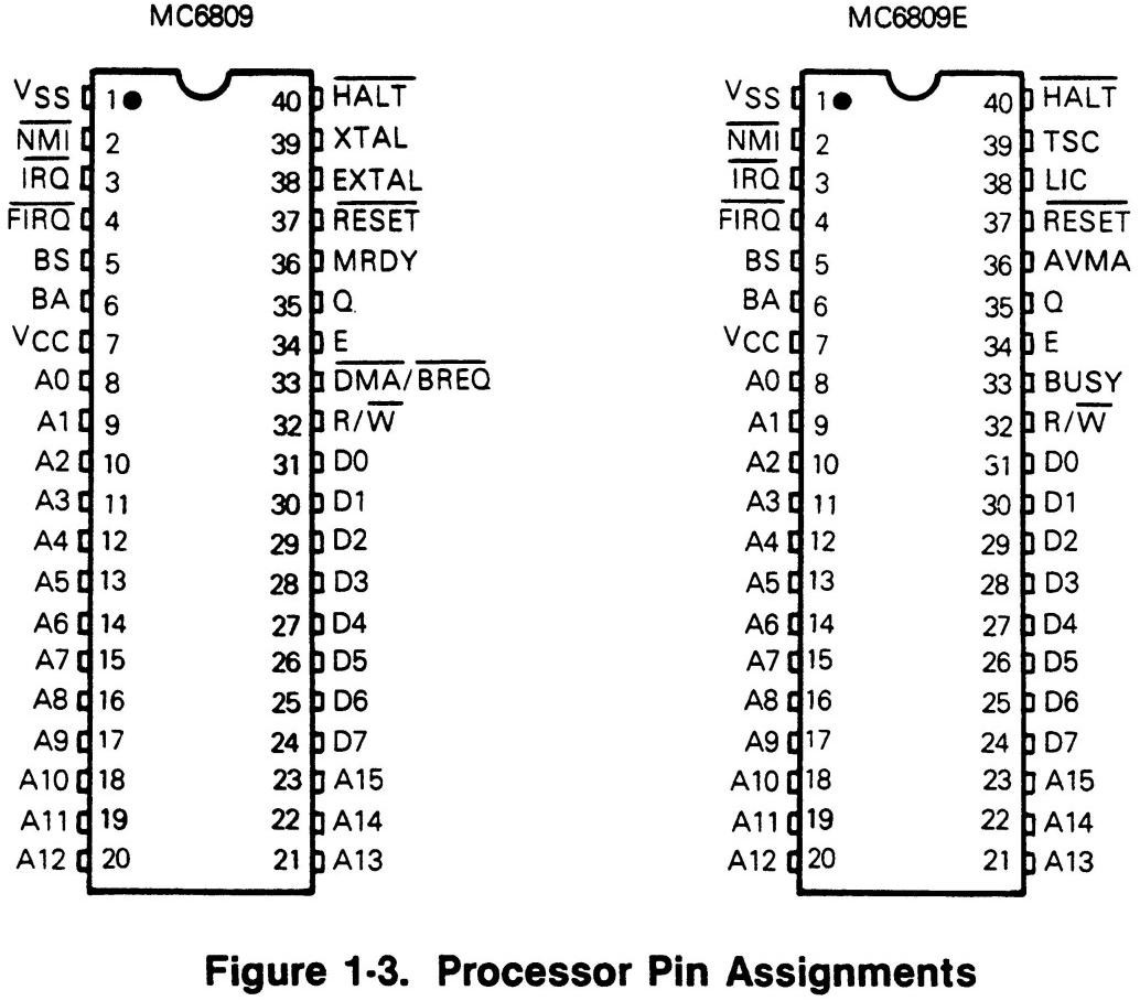
Its important to talk about the different types of 6809's. As far as I can tell there are 3 speed grades B, A and standard (68B09, 68A09, and 6809) these versions have a "On chip Clock Circuit". Additionally, there is a E variety that brings the divided clock outside of the chip. This computer uses the on chip clock variety. By way of comparison, the Tandy Color Computer (CoCo) uses the E variety All of these chips end with E[Package Type] and so they would be: 6809E, 68A09E, or 68B09E. The package type labeling varies but simply put P = plastic or C = Ceramic, and vice versa. Also, as a word of caution, it is easy to confuse the chips as they are all 40 pin packages but the pin outs are greatly different. There is an adapter available although I've not tried it and have no idea if it works well. Here's a cross reference of the CPU's I shamelessly ripped from google image search from this source:
The plan:
I'd like to build a basic computer (at first, though I'm not limiting myself). I'll base the initial build off of Grant Searle's 6809 basic computer. If you've never been over to his website you really should its an invaluable resource. A while back i built a terrible first attempt PCB of his keyboard and TV interface.... i'll not link it here as it's not a very good example of the design but if you look hard enough I'm sure you can find it.
Grant has spent a lot of time and energy on his website, so if you want schematics for his original build, he's asked everybody to not re-post them so head on over there to take a look.
To start I would like to improve the clock circuit. Since the chip has an internal crystal oscillator amplifier pin (XTAL), grant simply used it with a crystal and two capacitors. This arrangement is actually specified in the datasheet, however, since there are 3 speed grades of the 6809 (non-E Version) it is nice to have a little divider circuit so that we can use the lowest and highest speed grade with a jumper and 1 crystal. Since were using an ACIA as a the initial display and user input interface, it is fortunate grant selected a 7.3728 Mhz crystal for his design. Simply, with that clock frequency we can get a baud rate of 115200 out of the AICA. However, by building a clock that can both supply a perfect clock for the serial interface and also optionally divide itself down to provide something closer to 4 Mhz ( ~3.68 Mhz), we can use the lower speed grade chip without harm. Additionally the CPU divides down the clock further, by a factor of 4. So in the end we get approximately 1.8 MHz. for a B speed grade chip and .9 Mhz for a standard 6809 (this sounds slow but compared to chips of the day it's actually right in there).
Since grants design, does not have (or really need for that matter) a power on reset, I had to add one for the clock divider in my clock. And so I went with the standard, substandard, C64 Reset Circuit:
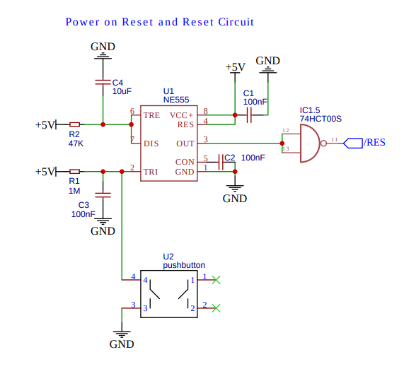
For the simple reason I've used it before, and it works. I may experiment with one of those reset chips, that provides watchdog / brownout protection, but for now this is a very common known design. Since I had to put in the inverter chip any way (actually its a NAND), I used two more gates to build a more standard clock Circuit:
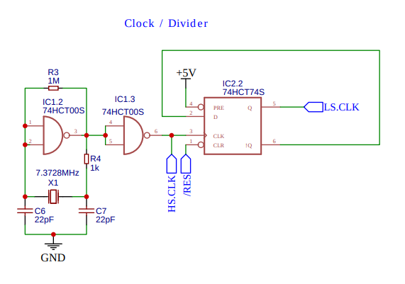
This gives me 2 clock Signals I can select for the main system clock, and a High speed (full speed) clock for the AICA (or really other peripherals that might need it.) I added a jumper block to the schematic with a PCB footprint so I can pick between the two for the main system clock if I decide to have PCB's made, at this point were just building on a bread board. Using this single pin configuration, the data sheet specifies we can ground the XTAL pin and connect a TTL compliant clock source to the EXTAL pin, so when I do the CPU module I will need to take this into consideration. The biggest concern is keeping the clock lines VERY short to prevent ringing; I may need to attenuate them if this becomes a problem.
Discussions
Become a Hackaday.io Member
Create an account to leave a comment. Already have an account? Log In.
A couple of thoughts:
- The /RESET input on the 6809 is a Schmitt-Trigger, so power on reset can be accomplished with just a resistor (to +5V) and capacitor (to GND).
- Unless you have reason to roll your own crystal oscillator, you can simplify things by just using a standard clock oscillator like the ECS-100AX-073.
- When drawing your schematics, GND shouldn't point up. It's just confusing if it does.
- Hou might want to take a look at this 6809-based project for additional ideas: MC6809-Based Arcade Game | Hackaday.io
Are you sure? yes | no
Thank you for the advice tips! I'm a novice (if it isn't obvious) I can certainly make the changes to the ground symbols. I did need a external power on reset for the clock divider, which is why I Built that. Honestly I have the crystals on hand so that's the reason I built it that way. I'll take a look at the arcade build a little while later. Thanks again :)
Are you sure? yes | no
Had a look at the design for the arcade build. I especially like the ability to swap out the CPU for a internal / external clock types without much hassle. Very interesting design 👍
Are you sure? yes | no