• Schematic

    kaimac5 days ago 0 comments

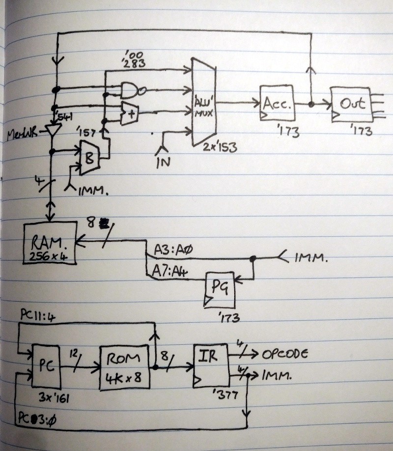
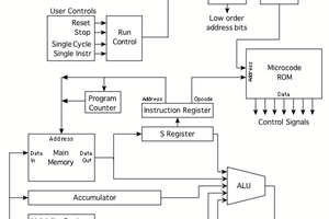
    Here is the schematic. All that is missing is the clock, some buttons connected to the input port and the display connected to the output port.

    There are 18 ICs in total, including RAM and ROM.

    Data stuff:

    Instruction stuff:

  • Multiplication

    kaimac08/04/2026 at 01:00 0 comments

    More programming.

    I looked at using the carry out from the adder but it's not worth it. It doesn't really simplify the subtract/compare code at all, because (A-B) = (A + ~B + 1), and that "1" causes problems if you don't have a carry in. Besides I prefer "jnz" to "jc" as a conditional branch.


    I fleshed out the assembler so you can define constants for memory locations etc. This makes the code significantly more readable and easier to write. I've also changed the names of some instructions to separate out the immediate/memory instruction types.


    Here's some code to multiply to 4-bit values into an 8-bit result. The next thing to look at will be driving the OLED display.

    Read more »

  • First real program

    kaimac07/31/2026 at 23:50 0 comments

    I sat down and wrote some assembly, to see what the CPU is like to program.

    I wrote a very simple simulator in Python that interprets the .asm file directly. Then I wrote this program, which outputs all the prime numbers less than 256. It's about 200 lines long, and it executes 3.1 million instructions before it finishes. 

    Doing loops and incrementing counters etc. is nice and straightforward. The addressing modes for the accumulator instructions feel nice, with them all being able to take an immediate value or use a memory location. That's the part of the ISA I'm most happy with. The NAND instruction is quite easy to use - you can NOT the accumulator easily with "nan f", and you can test specific bits easily with nan and jnz. I've only used one page of memory so not looked at the page setting instructions yet.

    Most of the program is spent doing 8-bit subtracts and compares, and most of that code is spent generating carry bits. It's quite fiddly and I think there's probably a bug in my compare code, although it works for this program. Obviously it's a very rudimentary 4-bit CPU so doing multi-word arithmetic is never going to be fun, but it has got me thinking whether I should try and use the carry output of the 283 adder somehow.

    Also the usual thing I find with writing assembly - coming up with label names that don't end up as nonsense is hard...

    Full program below:

    Read more »

  • Reviving the project

    kaimac07/31/2026 at 12:13 0 comments

    Hello everyone, coming back to this after several years :)

    As a reminder here is our instruction set:

    0000 iiii    lda i     acc = i
    0001 aaaa    lda $a    acc = mem[PG,a]
    0010 iiii    nan i     acc = acc NAND i
    0011 aaaa    nan $a    acc = acc NAND mem[PG,a]
    0100 iiii    add i     acc += i
    0101 aaaa    add $a    acc += mem[PG,a]
    011x xxxx    in        acc = in
    1000 iiii    spg i     PG = i
    1001 xxxx    pga       PG = acc
    101x aaaa    sta $a    mem[PG,a] = acc
    1100 iiii    out i     out = i
    1101 xxxx    out       out = acc
    1110 cccc    jnz $abc  jump if acc not zero ($ab in next byte)
    1111 cccc    jmp $abc  jump unconditionally ($ab in next byte)

    • There are four instructions that write to the accumulator: lda (load), nan (nand), add, and in. lda, nan and add can take a 4-bit immediate, or a 4-bit memory address in the current page.
    • The page register (the upper 4 bits of the 8-bit memory address) can be loaded from the accumulator with pga, or from an immediate with spg (set page).
    • Similarly the output register can be written with an immediate or from the accumulator
    • The accumulator can be stored at a memory location in the current page with sta.
    • There's one conditional jump: jump if accumulator not zero. And there's an unconditional jump. Jump instructions take a full 12-bit instruction address.

    The instruction decoding is very simple, just 3 ICs and some diodes that replace some AND and OR gates (got to keep the chip count down!). The instruction set does have some limitations, but I see these as only adding character to the software:

    • You can only jump to an immediate address, so if you want to implement subroutines, you will have to set a memory location to a unique value at each call site, and the subroutine will check this value to jump back to the right place. Very janky, but the whole CPU is janky so I kind of like it.
    • You can only store to an immediate address in the current page. But you can set the page register from the accumulator, so some indirection is possible. For example if you wanted to have an array of values, it would have to be stored at the same location across pages (e.g. 0x00, 0x10, 0x20...). Fun!

    There is some free space in the instruction set ("in" and "sta" both take up two opcodes to simplify the decoding, and "in" and "out" both have operands which are ignored). It's really tempting to try and add something extra, but I can't see an easy way of doing it.

  • A couple of changes

    kaimac11/23/2022 at 22:13 1 comment

    I made a couple of changes:

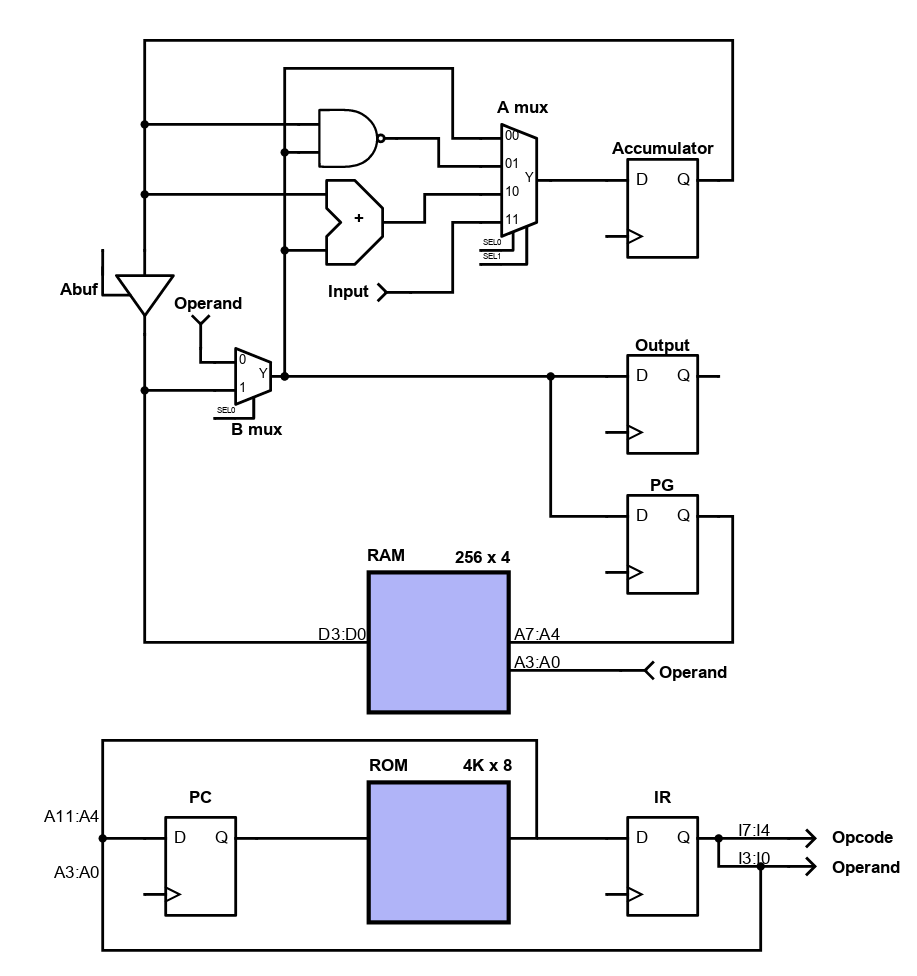
    • The page register PG is set via the B mux, so it can be set to a literal or to the accumulator value via ABuf.
    • Same with the output register
    spg 3     ; set page register to 3
    pga       ; move accumulator value to page register
    out 5     ; set output register to 5
    out       ; move accumulator value to output register

    These changes will add some functionality while simplifying the instruction decoding - always nice when that happens!

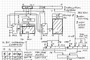
    To make this diagram I tried using Digikey's online schematic tool. The end result isn't too bad but it's not particularly nice to use. If anyone has any good suggestions for tools for making this kind of block diagram, please let me know!

  • Update

    kaimac11/21/2022 at 19:30 1 comment

    Here's where the design is at the moment:


    The accumulator (A) can take the value B, A+B, A nand B, or IN, where B is either a 4-bit immediate, or a 4-bit value from RAM. The accumulator can be sent to an output register, or written to RAM.

    The 8-bit RAM address is generated from 4 bits in the instruction word, and 4 bits from a page register (PG). So there are sixteen pages, each 16 words (nibbles) in size - an address of $3F is location F on page 3.

    In the diagram I've got the input to PG coming from an immediate value, but thinking about it now, why doesn't it come from the accumulator? Then you can compute page addresses and have some indirection. The only reason I can see for not doing that is that you can't have a value in the accumulator and then save it to a specific 8-bit address - you need to clobber the accumulator to update PG. But you could save it temporarily to the current page - perhaps location 0 of each page is kept free for such a thing. More thinking is necessary here - a lot of this stuff has been paged out of my head.

    Instructions come from a 4K ROM and are 8 bits wide. The 4-bit operand is either an immediate value or a RAM location. Or - in the case of a jump - the lower 4 bits of the 12-bit jump target. So where do the other 8 bits come from? They come from the next location in ROM, which handily is already available - it's the input to the instruction register rather than the output. All thanks to the "pipelined" nature of instruction fetching. The jump logic will be the topic of the next update.

  • Adding without carry

    kaimac08/28/2022 at 16:43 3 comments

    It would be nice to be able to make use of the carry output from the 74LS283 adder, but it's going to require at least one extra chip to store the carry bit, and maybe more to decode the opcode into a "write carry" signal.

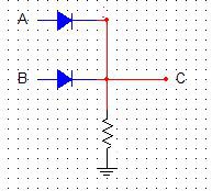
    The alternative is to OR all the accumulator's bits together to test for zero. That doesn't need any chips, just four diodes connected like this:

    "jnz" (jump if accumulator is not zero) will be our conditional jump.

    The question now is, how do you synthesise a carry bit in software if you don't have one in hardware? I couldn't find much information about this - a common definition of the carry bit is "1 if the result of A+B is less than A (or B)", but that's not very helpful - it's not very easy to do an unsigned comparison without a carry flag! In the end I found the answer in the source code for the Gigatron, which I knew doesn't have a carry flag.

    Q = A + B
    if top (sign) bit of Q is set:
      carry bit = top bit of (A & B)
    else:
      carry bit = top bit of (A | B)

    This is where having a NAND operation becomes very useful. ANDing A and B is just a case of NANDing, then inverting:

    lda $A
    nan $B
    nan f    ; nand with 0b1111 = invert
    

     OR is ~(~A . ~B), i.e. NAND with both inputs inverted. This requires a temporary location:

    lda $A
    nan f
    sta $notA
    lda $B
    nan f
    nan $notA     ; ~A nand ~B == A or B

    Putting it all together, here's how to add two 8-bit numbers:

    ; input values
    
            lda f       ;a=0xff (big endian, stored at $0/$1)
            sta $0
            lda f
            sta $1
            
            lda 5       ;b=0x52 (stored at $2/$3)
            sta $2
            lda 2
            sta $3
    
    ; add two 8-bit numbers
    
            lda $1      ; add lo nibbles
            add $3
            sta $5      ; store result at $5
            nan %1000   ; check hi bit
            nan f
            jnz set
            lda $1      ; msb clr: a or b
            nan f
            sta $f          ; $f = not a
            lda $3
            nan f
            nan $f
            jmp next
    set:    lda $1      ; msb set: a and b
            nan $3
            nan f
    next:   nan %1000   ; hi bit is carry
            nan f
            jnz carry
            jmp addhi   ; acc already zero if no carry
    carry:  lda 1
    addhi:  add $0      ; add hi nibs + carry
            add $2
            sta $4      ; store result at $4

  • ALU

    kaimac08/28/2022 at 15:47 0 comments

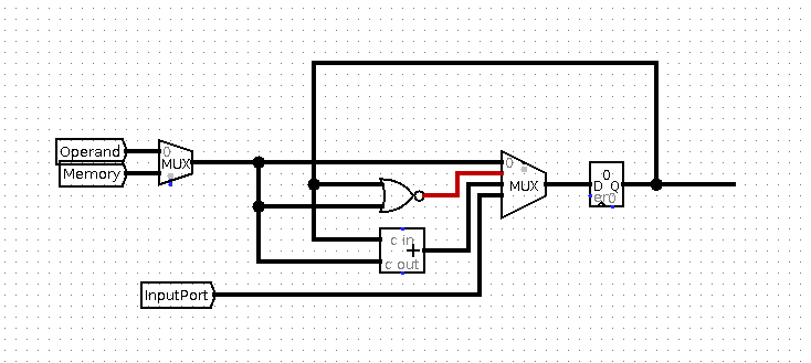
    Here is what I am thinking of for the "ALU":

    • We need a way to load the accumulator with an immediate value ("lda 3"), or from a memory location ("lda $3"), so a mux is required there.
    • At a minimum we want to be able to add a value to the accumulator. We already have that mux so the value could be immediate or direct. Another mux is needed to select between "add" and "load". The input port can also feed into that mux.
    • At the cost of one extra chip, a logic function will be very useful. I've put NOR in the diagram but after playing around I think NAND is slightly more useful (easier to do AND for testing bits).

    That allows for these instructions: 

    000m vvvv  lda    acc = value
    001m vvvv  add    acc = acc + value
    010m vvvv  nan    acc = ~(acc & value)
    011x xxxx  in     acc = in
    
    m: 0=immediate value, 1=value from given RAM address
    v: 4-bit value
    x: don't care

      
    I really like how this turned out, because the decoding for these instructions requires no additional chips!

    opcode bits:
       3210 vvvv
       ||||
       |||\- operand/memory mux select
       ||\-- accumulator source mux select
       |\---             -"-
       \---- accumulator write enable (active low)
    

    Two opcodes are taken up by "in" but it's worth that small cost.

  • Initial thoughts

    kaimac08/21/2022 at 15:28 0 comments

    • Tiny 4-bit CPU with 4-bit input and output ports. Like the #TD4 CPU but a bit more capable.
    • Connect the output port to a SSD1306-style OLED display. These can be driven via SPI which would be simple enough.
    • Have it do something non-trivial - I love the TD4 for its simplicity, but can a slightly more capable CPU do something more interesting? How about finding prime numbers, or displaying a fractal?
    • 256 words of RAM is plenty. It will have to be a Harvard architecture with a considerably bigger program ROM - 4Kx8 sounds good. Instructions would be 8 bits wide.
    • As few ICs as possible. The TD4 has 12 chips, but can only run very small programs. This Brainfuck machine has 14 chips and can run non-trivial programs, but you need to be a wizard to write programs for it. Let's see what can be done with less than 20. Instruction decoding can be done with the help of diodes.

    If we're going to write characters to the display we need a font, which is a lot of constant data. The easiest thing is for that constant data to reside in ROM in the form of instructions, which populate RAM:

        lda %1011    ; load accumulator with 4 bits
        sta $1       ; store at some memory location (upper 4 address bits will come from somewhere else)
        lda %0101    ; next 4 bits
        sta $2
        ...

     The next part of the program then reads the data in RAM and clocks it out serially.

    Control flow: we will have something simple like "jump if accumulator is zero". Is this enough? Can you have subroutines when you can only jump to an immediate address? Maybe if you have a jump table at the end of each subroutine, selecting which caller to jump back to.

    Addressing: similar question - can all addresses be immediate, or do we need the ability to store addresses in RAM?

    There will be many tradeoffs to look at - if removing a couple of chips causes the code size to balloon to make up for it, it may not be worth it.