Close
0%
0%

FPGA NES

Learning Verilog by creating an FPGA implementation of the Nintendo Entertainment System

Similar projects worth following
FPGA implementation of the Nintendo Entertainment System

My goal with this project is to learn FPGA design by implementing an original Nintendo Entertainment System (North American, not the Famicom) in Verilog. I'm still working out details of implementation (A/V peripherals, memory, user interface, etc), but I have a few design choices already made (mostly purely arbitrarily).

Language: Verilog. No real reason for this choice, I used VHDL in college a bit and thought Verilog seemed neater.

Hardware platform: I'm using the Mimas V2 FPGA development board from Numato Lab (http://numato.com/mimas-v2-spartan-6-fpga-development-board-with-ddr-sdram/). I mostly bought it because it was cheap and had a bunch of peripherals baked in already. It uses a Xilinx Spartan 6, which seems more than big enough for now, and has some nifty things built-in like a 512 Mb DDR RAM, USB support for programming and communication, and VGA and audio outputs (along with the standard buttons, switches, LEDs, and GPIOs). I've already run into at least one glitch, which I'll discuss later, but overall I've been pretty pleased with it.

Software platform: I'm using the ISE Webpack IDE from Xilinx as the synthesis, implementation, simulation, and compilation toolchain. Numato also has a custom executable for downloading the generated FPGA configuration file to the board through USB, which is handy. ISE has given me some trouble already, I think mostly due to its lack of Windows 10 support, but I've figured out workarounds to most of them and I'm too lazy to do anything about it. I've also written a few supporting programs for communication with the board in Java (using NetBeans, because reasons).

Shortly, I'm going to start uploading build logs to document what I've done so far (as of this writing, I've implemented the CPU and am doing some testing of it now). I hope to pretty thoroughly explain what I'm doing in each part, both so people can check me on it, and so I don't forget in like 6 months as usual.

If anybody sees this and notices any errors or Verilog/FPGA noob mistakes, please don't hesitate to let me know. I'm in this to learn things, and while I've tried to take care to do things in a semi-up-to-standard way, I have probably definitely 100% done silly things, and would like to correct them if possible.

Enjoy reading through this! All code is hosted on GitHub, there should be a link to it on this page somewhere.

  • ADC and Immediate Addessing

    irwinz05/08/2017 at 01:55 0 comments

    Now we’ll get into a concrete instruction example: ADC. This instruction will add a number to the accumulator register, and will then store the result back in the accumulator and set some flags based on the result. And we’ll start with one of the simplest addressing modes: immediate addressing. In this mode, the byte that you want to add is actually stored right next to the opcode in the program code (and was, in fact, hardcoded into the program as a constant), so that you just have to increment the program counter and fetch the byte. Since we have multiple addressing modes for this one instruction, we’ll denote this one “ADC_IMM” (for obvious reasons).

    Ok, so the operations that take place on each cycle are:

    Cycle 0: Fetch the ADC_IMM opcode
    Cycle 1: Fetch the byte to add
    Cycle 2: Add the byte to the accumulator, and fetch the next opcode
    

    Pretty simple, I suppose. Note that, since we’re fetching the next opcode at the same time that we perform the add, this instruction technically only takes 2 cycles (you can count cycle 3 as cycle 0 of the next instruction), which is the basis for the 6502’s pipelining. Now, we’ll look at how to translate those basic steps into actual CPU operations:

    case (cycle)
      0: begin
        case (IR)
    	ADC_IMM: begin  // next cycle: store ALU result, fetch next byte
    	  I_cycle <= 1;							// increment cycle counter
    					
    	  PCL_ADL <= 1; ADL_ABL <= 1; PCH_ADH <= 1; ADH_ABH <= 1;	// output PC on address bus
    	  I_PCint <= 1; PCL_PCL <= 1; PCH_PCH <= 1;			// increment PC
    				
    	  ADD_SB <= 1; SB_AC <= 1; SB_DB <= 1;				// move ADD to AC through SB
    	  AVR_V <= 1; ACR_C <= 1; DBZ_Z <= 1;	DB7_N <= 1;		// add result flags to status reg
    	end
        endcase
      end
      1: begin   
        case (IR)
            ADC_IMM: begin  // next cycle: ALU add, fetch next opcode
    	  R_cycle <= 1;							// reset cycle counter to 0
    							
    	  PCL_ADL <= 1; ADL_ABL <= 1; PCH_ADH <= 1; ADH_ABH <= 1;	// output PC on address bus
    	  I_PCint <= 1; PCL_PCL <= 1; PCH_PCH <= 1;			// increment PC
    							
    	  DL_DB <= 1; DB_ADD <= 1; AC_SB <= 1; SB_ADD <= 1; SUMS <= 1;	// perform ALU add on AC, DL
    	end
        endcase
      end
    endcase

    It may help if we start in Cycle 1, and if we ignore the last line. Actually, let's reformat a little bit:

    case (cycle)
      0: begin
        case (IR)
    	ADC_IMM: begin  // next cycle: store ALU result, fetch next byte
    	  I_cycle <= 1;							// increment cycle counter
    					
    	  PCL_ADL <= 1; ADL_ABL <= 1; PCH_ADH <= 1; ADH_ABH <= 1;	// output PC on address bus
    	  I_PCint <= 1; PCL_PCL <= 1; PCH_PCH <= 1;			// increment PC
    				
    	  ADD_SB <= 1; SB_AC <= 1; SB_DB <= 1;				// move ADD to AC through SB
    	  AVR_V <= 1; ACR_C <= 1; DBZ_Z <= 1;	DB7_N <= 1;		// add result flags to status reg
    	end
    
            PREV_OP: begin // next cycle: fetch next byte
              I_cycle <= 1;							// increment cycle counter
    					
    	  PCL_ADL <= 1; ADL_ABL <= 1; PCH_ADH <= 1; ADH_ABH <= 1;	// output PC on address bus
    	  I_PCint <= 1; PCL_PCL <= 1; PCH_PCH <= 1;			// increment PC
    	end			
        endcase
      end
      1: begin   
        case (IR)
            ADC_IMM: begin  // next cycle: ALU add, fetch next opcode
    	  R_cycle <= 1;							// reset cycle counter to 0
    							
    	  PCL_ADL <= 1; ADL_ABL <= 1; PCH_ADH <= 1; ADH_ABH <= 1;	// output PC on address bus
    	  I_PCint <= 1; PCL_PCL <= 1; PCH_PCH <= 1;			// increment PC
    							
    	  DL_DB <= 1; DB_ADD <= 1; AC_SB <= 1; SB_ADD <= 1; SUMS <= 1;	// perform ALU add on AC, DL
    	end
    
            PREV_OP: begin // next cycle: fetch next opcode
              R_cycle <= 1;							// reset cycle counter to 0
    							
    	  PCL_ADL <= 1; ADL_ABL <= 1; PCH_ADH <= 1; ADH_ABH <= 1;	// output PC on address bus
    	  I_PCint <= 1; PCL_PCL <= 1; PCH_PCH <= 1;			// increment PC                                     
            end
        endcase
      end
    endcase

    Ok, now we'll start in Cycle 1, and we're currently executing the previous operation (so IR equals the cleverly named "PREV_OP" opcode). Here, the next cycle will be the last cycle of this instruction, so we need to go out and fetch the next opcode (which will be the ADC_IMM instruction). We're going to reset the cycle counter to zero (the R_cycle command). To fetch the...

    Read more »

  • Instruction Decoder

    irwinz05/03/2017 at 22:38 0 comments

    And we’re back! I debated whether to dive straight into the instruction decoder or to introduce the CPU registers and all of the bus connections first. I think I’m going to combine it though, and hopefully that won’t just confuse the issue. In this log, we’re going to go through the basics of the instruction decoder implementation, and then go into the first instruction addressing mode, and I’ll explain each register/bus as we get to it.

    So last time we talked about how each instruction takes some number of CPU cycles to complete, and on each cycle the decoder will control the rest of the CPU to perform some action. To implement that, the instruction decoder is set up as two nested case statements:

    module InstructionDecoder(
        input sys_clock, rst,   // main system clock and reset    
        input clk_ph2,          // clock phase 2    
        input [2:0] cycle,      // current instruction cycle
        input [7:0] IR,         // instruction register
        output reg CTRL_SIG1    // output control signal(s)
        );
    
    // Decode current opcode based on cycle:
    always @(posedge sys_clock) begin
    
        if (rst == 0) begin
            // Reset control lines
            CTRL_SIG(s) <= 0;
        end
        else if (clk_ph2) begin
            // Reset all control lines by default so we don't forget any
            CTRL_SIG(s) <= 0;
            
            // Switch on cycle first, then opcode (will determine what happens on the NEXT cycle):
            case (cycle)
                0: begin
                    case (IR)
                        opcode1, opcode2: begin
                            // set up CPU for cycle 1 operations
                            CTRL_SIG(s) <= x;
                        end
                        opcode3: begin
                            // set up CPU for cycle 1 operations
                           CTRL_SIG(s) <= x;
                        end
                    endcase
                end
                1: begin
                    case (IR)                     
                        opcode1, opcode2: begin
                            // set up CPU for cycle 2 operations
                            CTRL_SIG(s) <= x;
                        end
                        opcode3: begin
                            // set up CPU for cycle 2 operations
                            CTRL_SIG(s) <= x;
                        end                
                    endcase
                end
            endcase
    
        end
    
    end
    endmodule
    
    // Opcode definitions
    localparam [7:0] opcode1 = 8'hxx, opcode2 = 8'hyy, opcode3 = 8'hzz;
    

    As you can see, the decoder takes the clocks, instruction register, and current CPU cycle as inputs (actually, it will have more, but we’ll get there), and will output various 1-bit control signals which will be sent to the various parts of the CPU.

    The control signals will be updated on each phase 2 clock. The outside case statement switches on the CPU cycle, while the nested case switches on the opcode (I think the opposite way would be easier to track each instruction, but this way should be less redundant since a lot of opcodes do the exact same thing on each cycle). One important thing here is that you’re actually setting up the operations that will take place on the next cycle, since we’re on phase 2 now (side note: this was, for some reason, stupidly hard for me to wrap my tiny brain around, so it took forever to get the first opcode done). And finally, to make things easier to read, we’ll create a list of local parameters which are just human readable names for each opcode.

    I should also mention that this point (if not earlier…) that most of the 6502 instructions have multiple addressing modes, and each one of these addressing modes has a separate opcode. So if you want to load in a byte from memory, for example, there are up to 8 different ways of telling the CPU where that byte is in memory. It can get super confusing, but this actually means that all of the opcodes with a certain addressing mode are 90% identical – the hard part is figuring out how to calculate the address, but once you have it then the actual operation is pretty simple.

    So that’s the general outline of the decoder. Next log, we’ll get into concrete examples (wooo, you say).

  • Instruction and Cycle Controller

    irwinz04/30/2017 at 20:14 0 comments

    So we’ve talked about how to keep track of where we are in a program, but we haven’t talked about how we actually decide which parts of memory are actual opcodes, which are operands, and which are just data. That’s a pretty involved process, so we’ll split it into 2 parts and here we’ll talk about the basics of how instructions are executed and how they get loaded into the CPU (we’ll save the actual interpretation of those instructions for later). To start, here’s the block diagram for loading instructions:

    Starting from the top, we’ve got the external data bus which shuttles data between the CPU and memory (it’s a tri-state bus that can both read and write, but we’ll ignore the writing part for now – so for this post, it’s just a data input bus). Next, we have the pre-decode register, which gets loaded with the contents of the data bus on every phase 2 clock. Note that that’s every phase 2, so it’ll get loaded with junk a majority of time and we have to figure out when it’s not junk. Next we’ve got some pre-decode logic, whose main function is to replace the pre-decode register data with a pre-determined opcode during an interrupt. We’ll get to interrupts later, so just remember this part and, for now, ignore it. Finally, we have the brains of the thing: the instruction register and the timing logic.

    First, some basics: every instruction takes some number of CPU cycles to complete (remember that 1 cycle is made up of a phase 1 and phase 2 clock). To determine what happens on every cycle of the current instruction, the instruction decode logic must take into account both the current opcode and the current cycle. However, the number of cycles per instruction varies, and isn’t necessarily fixed even for a single instruction (things like branches take a variable amount of cycles, for example, and even accessing memory in certain locations can add cycles as we’ll see later). So the decode logic also needs to control the timing logic in order to keep everything synced up, and we get a big feedback loop.

    Now with that basic idea, we can get down to how it actually works. There are 8 cycles the CPU can be in (in the block diagram, there’s a T1X cycle for some reason, but my implementation just goes from 0 to 7 like a normal person). The longest instructions only take 7 cycles to complete, but there are 8 labels since a few instructions can skip a cycle (to be explained later). Anyway, every instruction is set up to fetch the next opcode during the 0th cycle. So during the 0th cycle, the CPU will send out the address of the next opcode during phase 1, then the fetched data is latched into the pre-decode register on phase 2. Then, that data is finally latched into the instruction register on the following phase 1 (of the 1st cycle). This all works because each instruction knows when it's done and should fetch the next opcode, and if it was implemented correctly, the program counter will be pointing at the next opcode.

    Ok, well, that was a lot of background for a pretty straightforward thing, so here’s the code!

    module InstructionController(
        input sys_clock, rst,	     // Main system clock and reset
        input clk_ph1,		     // clock phase 1
        input [7:0] PD,		     // pre-decode register
        input I_cycle, R_cycle, S_cycle, // increment/reset/skip cycle counter lines
        input int_flag,                  // perform interrupt
        output reg [7:0] IR,             // instruction register
        output reg [2:0] cycle,          // current instruction cycle
        output [2:0] next_cycle          // next instruction cycle
        );
        
    // Signal declarations:
    wire [7:0] opcode;      // Opcode to put into instruction register
        
    // Decide what the next cycle count should be:
    assign next_cycle = (R_cycle == 1) ? 3'd0                                             // if reset_cycle, reset count to 0
                                       : (I_cycle == 1) ? cycle + 3'd1                    // else, if increment_cycle, increment count
                                                        : (S_cycle == 1) ? cycle + 3'd2   // else, if skip_cycle, increment count twice
                                                                         : cycle;         // else, don't change count
        
    // Decide what gets loaded into the instruction register (change only on T1 cycle):
    assign opcode = (next_cycle...
    Read more »

  • Program Counter

    irwinz04/29/2017 at 22:00 0 comments

    Next up, we’ve got the 6502 program counter! The PC is going to keep track of where we are in the program at any given time. Because the 6502 has a 16-bit address space, the PC has 2 8-bit registers for the low and high byte, respectively (it has 2 separate registers instead of 1 16-bit register, because some of the addressing modes handle the low byte separately - we'll get into this later). The operation of the PC is fairly straightforward, it gets loaded with a particular value, and then will increment that value as the program progresses (controlled by the cycle/opcode decoder mentioned last time). I’ve added the block diagram below to show the registers and inputs/outputs:

    It looks a bit complicated, because (a) you have to have some logic to increment the high byte when the low byte overflows, and (b) there are a couple of input/output choices to load and shuttle the PC around as needed. For (b), you can load the PC with either the current PC value (to simply increment to the next byte), or with the contents of the address buses (low byte, high byte, or both). If you’re wondering what the deal is with the high-byte incrementer being split into bits 0-3 and 4-7, you’re not alone. I still am not sure what that’s for… anybody got some clarification? Ah well, we’ll just ignore it for now. Here’s some code!

    module ProgramCounter(
    	input wire sys_clock, rst,         // Main system clock and reset
            input wire clk_ph2,                // Phase 2 clock enable
    	input wire [7:0] ADLin, ADHin,	   // Address Bus low & high bytes
    	input wire INC_en, 		   // Increment PC enable
    	input wire PCLin_en, PCHin_en,	   // Use current PC
    	input wire ADLin_en, ADHin_en,	   // Load new value into PC
    	output wire [7:0] PCLout, PCHout   // PC Bus output
        );
    	
    
    // Declare signals:
    reg [7:0] PCL, PCH;		// PC register low & high bytes
    reg [7:0] PCLS, PCHS;		// PC select register low & high bytes
    reg PCLC;			// PC low-byte carry bit (to increment high-byte)
    reg [7:0] PCL_inc, PCH_inc;	// Incremented PC
    
    // Select PC source: previous PC or new value from Address Bus:
    always @(*) begin
    	
    	if (PCLin_en)
    		PCLS <= PCL;		// load previous PC register value
    	else if (ADLin_en)
    		PCLS <= ADLin;		// load address bus value
    	else
    		PCLS <= PCL;		// default: previous PC
    		
    	if (PCHin_en)
    		PCHS <= PCH;		// load previous PC register value
    	else if (ADHin_en)
    		PCHS <= ADHin;		// load address bus value
    	else
    		PCHS <= PCH;		// default: previous PC
    		
    end
    
    // Increment PC:
    always @(*) begin
    
    	{PCLC, PCL_inc} = PCLS + 1'd1;	// Increment low-byte with carry out
    	PCH_inc = PCHS + PCLC;		// Increment high-byte with carry from PCL
    	
    end
    
    // Latch PC on phase 2 clock:
    always @(posedge sys_clock) begin
    	
    	if (rst == 0) begin		// initialize PC to zero (will be replaced)
    		PCL <= 0;
    		PCH <= 0;
    	end
    	else if (clk_ph2) begin
    		if (INC_en) begin	// if Increment enabled, latch incremented PC
    			PCL <= PCL_inc;
    			PCH <= PCH_inc;
    		end
    		else begin		// else, latch passed-through value
    			PCL <= PCLS;
    			PCH <= PCHS;
    		end
    	end
    		
    end
    
    // Assign outputs:
    assign PCLout = PCL;
    assign PCHout = PCH;
    
    
    endmodule

    Ok, pretty straightforward here too. I’ve included the address bus as an input so we can grab the value as needed. I’m just including a single output for the current value of the PC, and we’ll let the instantiating module deal with shuttling it to where it needs to go. The module will select the input to the incrementer as either the current PC or the address bus, then will go ahead and produce an incremented value based on that (leaving the original unincremented, since we don’t know for sure whether we’ll be instructed to increment or not). Then, on phase 2 of the cycle, we’ll latch either the incremented or original value into the PC register for output.

    Hmmm, I guess I should talk about clocks… Right! So, first, all synchronous logic in the NES implementation runs off a single system clock to avoid timing issues (note that the ALU last time was purely combinational, with no clocks). Second, the 6502 actually...

    Read more »

  • ALU Implementation

    irwinz04/29/2017 at 16:52 0 comments

    Ok, here we’re going to go through the 6502 ALU (and my implementation of it), since it’s relatively straightforward and independent of the rest of the CPU. Below I’ve included the block diagram of the ALU.

    It’s got two 8-bit input registers (A and B), both of which can be filled from several different inputs. The B input can additionally be fed with an inverted data bus, allowing the ALU to do subtraction. There are 5 intrinsic operations: add, and, or, exclusive-or, and shift right. The add instruction can also do subtraction, when combined with the inverted data bus. There is a carry-in and carry-out, to allow for >8-bit operations. There is also an overflow bit that detects signed over- or underflow. On the block diagram there are a few other input and output bits, but those are used only for the 6502 decimal mode which the NES CPU does not implement, so we’ll ignore them.

    I won’t talk about the input or output registers here, as I decided to have the ALU module be independent of them. I included them in the diagram in order to highlight the inverted DB input. In my ALU, I moved the inversion into the ALU itself rather than outside the B input (because it was cleaner? I dunno, it just happened). So the inputs to the ALU module consist of the A and B registers, the carry bit, and the control signals (the operations plus the inversion signal). One final change is that I included an extra operation, rotate right. That was done purely for convenience, since I’m still not quite sure how this was implemented on the actual 6502 (can anybody clarify?).

    With that, here’s the code:

    module ALU(  
        input wire SUM_en, AND_en, EOR_en, OR_en, SR_en, INV_en, ROR_en, // Operation control
        input wire [7:0] Ain, Bin, 					     // Data inputs
        input wire Cin, 						     // Carry in
        output reg [7:0] RES,					     // Operation result
        output reg Cout, 						     // Carry out
        output wire OVFout						     // Overflow out
        );
    	
        // Declare signals:
        wire [7:0] Bint;
    	 
        // Select inverted or non-inverted B input:
        assign Bint = INV_en ? ~Bin : Bin;
        
        // Perform requested operation:
        always @(*) begin
    	 
    	// Defaults:
    	RES = 0;
    	Cout = 0;
    		
    	// Operations:
            if (SUM_en)
    	    {Cout, RES} = Ain + Bint + Cin;	// add with carry-in, carry-out
            else if (AND_en)
                RES = Ain & Bin;			// and
            else if (EOR_en)
                RES = Ain ^ Bin;			// xor
            else if (OR_en)
                RES = Ain | Bin;	                // or
            else if (SR_en)
                {RES, Cout} = {Ain,1'd0} >> 1;	// shift right with carry-out
    	else if (ROR_en)
    	    {RES, Cout} = {Cin,Ain,1'd0} >> 1;	// shift right with carry-in, carry-out
    		
        end
    	
        // Set overflow flag (set if both inputs are same sign, but output is a different sign):
        assign OVFout = (Ain[7] && Bint[7] && (!RES[7])) || ((!Ain[7]) && (!Bint[7]) && RES[7]);
    	 
    endmodule

    As noted above, the B input inversion in handled inside the ALU module, for reasons. Each operation is handled in a separate case. The input carry bit is used for add and rotate right operations. Carry output is changed for add, shift, and rotate operations (auto cleared for logical ops, but the rest of the CPU will ignore it in those instances). The overflow bit is an interesting one (the best reference for understanding it is Ken Shirriff’s blog: http://www.righto.com/2012/12/the-6502-overflow-flag-explained.html), it basically detects when an operation results in a number that can’t fit in a signed byte (for example: 127 + 1 = -128, instead of +128). To calculate it, the ALU checks that if both inputs (after inverting B if necessary) are the same sign, the result should also be that sign. If it’s not (again, +127 + 1 = -128), then the overflow bit is set. By inverting B, the same math works for subtraction and negative inputs.

    One note here is that the ALU relies on the programmer to correctly set the carry input for the requested operation. For example, for a normal 8-bit add, the carry bit should be cleared before the operation (for >8-bit adds, the carry is cleared for the first op, and then the carry out is used for the next byte(s))....

    Read more »

  • CPU overview

    irwinz04/29/2017 at 15:19 0 comments

    Ok, first post! So far, I’ve implemented the CPU and absolutely nothing else, so here we’ll go through a super quick overview of the NES CPU and then get into details of the code in further log posts. The CPU has been previously documented way more thoroughly than I could ever do (see, for example, the good folks over at http://wiki.nesdev.com/w/index.php/NES_reference_guide), so we’ll keep this brief.

    The NES CPU (the Ricoh 2A03) used a variant of the 8-bit MOS 6502 processor as its core (the 2A03 contains the 6502 core along with some I/O registers and an audio processor). The only difference in the Ricoh 6502 and the original MOS 6502 is that the former lacks the decimal mode found in the original, so the real work here is implementing the 6502.

    The main references I used were Donald Hanson’s block diagram of the 6502 and the MOS programming and hardware manuals (see the “Docs” folder on the GitHub repo). Well, those along with the literally thousands of pages of information on the NesDev wiki/forum and elsewhere on the web (also, a shoutout to another NES FPGA implementation from Brian Bennett, which helped me out more than a few times when I was stumped - https://github.com/brianbennett/fpga_nes). I’m going to throw the 6502 block diagram in here for reference, since things make a lot more sense (to me, anyway) looking at it.

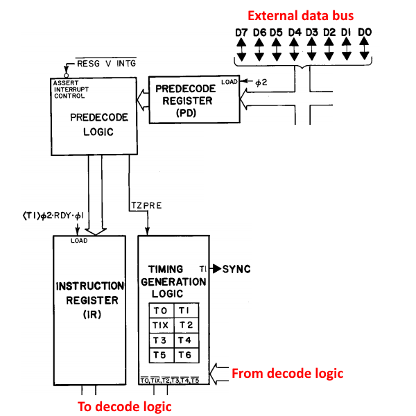
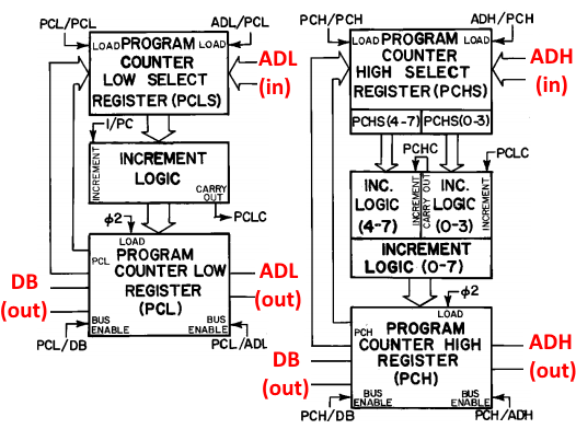
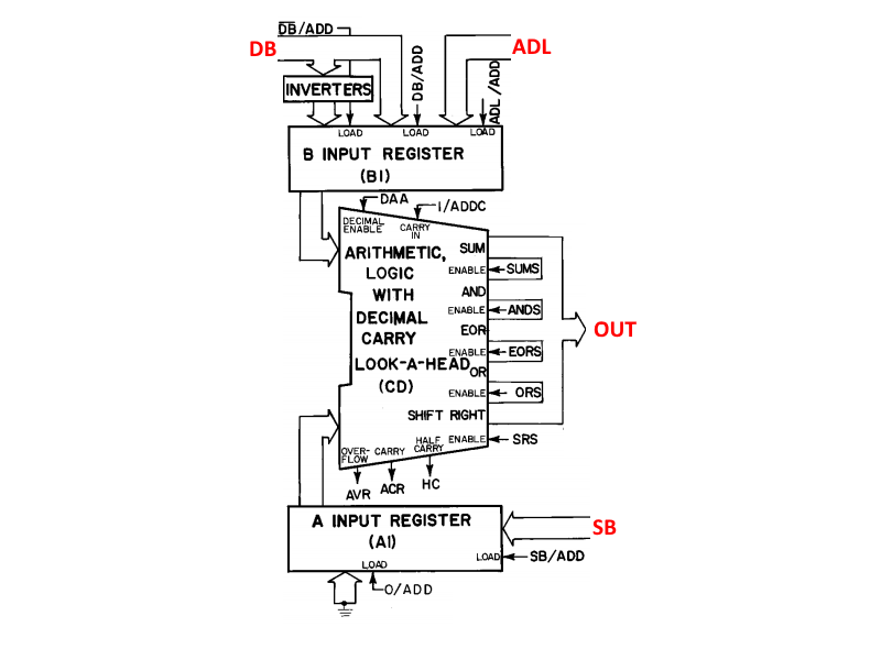
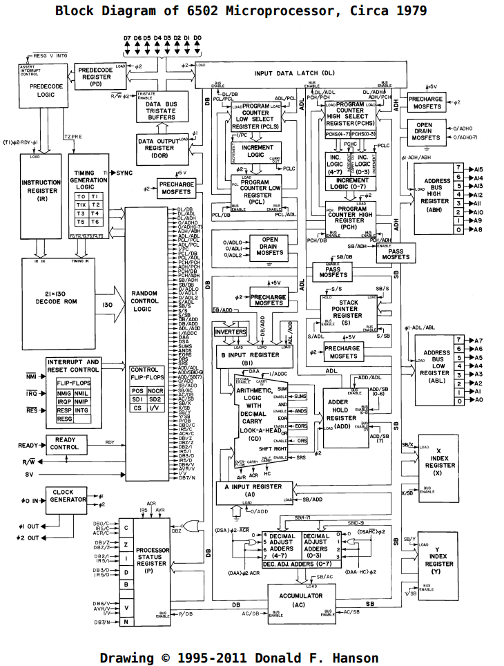
    Some basics: The 6502 is an 8-bit processor, with a 16-bit address space. It has 6 internal registers (3 special purpose – the program counter, status register, and stack pointer – and 3 general purpose – X, Y, and the accumulator). The registers are linked to the various parts of the CPU through 2 main internal buses (the Data Bus and the Special Bus, DB and SB in the block diagram), along with 2 buses dedicated to shuttling the low and high bytes of the address around (ADL and ADH in the block diagram). There are also interconnects between buses so you can connect them together and get data wherever it’s needed. The ALU is pretty central in the design: besides the usual operations on external data, it’s also used for internal purposes like temporarily storing data and addresses while other data is being fetched as well as computing addresses for some of the more complicated addressing modes. All of this is coordinated and controlled via the opcode decoder, which decides what to do on each cycle of each opcode.

    Ok, that probably explained exactly zero, but we’ll leave it there for now. In the next log, I’m going to start explaining the ALU and my implementation of it.

View all 6 project logs

Enjoy this project?

Share

Discussions

Similar Projects

Does this project spark your interest?

Become a member to follow this project and never miss any updates