 Yann Guidon / YGDES
Thank you CircuitJS !
Play at home with this link.
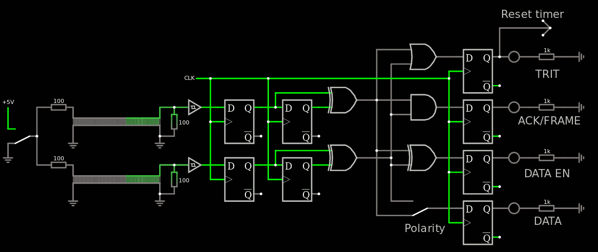
I use the delay lines to simulate imperfection and transmission delays, and also implement sending 0s and 1s. The simultaneity is a very important aspect because a mismatch deteriorates the data. In SW there is little trouble, usually. In HW it's a bit more complex and I'll have to find a better way than the one above.
It's basically a clock domain crossing issue, right ? At least I implemented a first "buffer" DFF to prevent metastability but this is not totally foolproof. Jitter during ACK can last a whole clock cycle but can't cross cycles, so it's only half perfect.
If you change the delay of one delay line, the circuit will receive a 0 then a 1, or vice versa. I added a "polarity" selector "in case the data lines are swapped. This can be implemented by a MUX or XOR with a DFF, itself initialised "as it should" and updated by a service message.
Remember : the above circuit is only a proof of concept and does not address inter-signal jitter properly. But it shows the basic ideas, and I could start implementing a basic sender.
.................
This one should work better !
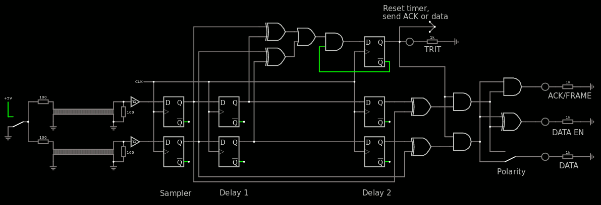
The tolerance to inter-wire jitter is increased because the data is XORed with 2 clock cycles of delay. The first delay detects "a transition" with an anti-double-trigger loopback (in green).
Normally we could increase the tolerance by XORing the data at the outputs of the Schmitt triggers, because the signal should not change once one transition is detected, but it's a detail to manage later.
Here is the source code.
Discussions
Become a Hackaday.io Member
Create an account to leave a comment. Already have an account? Log In.