 Lithium ION
555 timer is one of the most advanced and most popular IC of it’s time. This IC has a lot of configurations and circuit arrangements. We can design some small sections of a circuit using this IC without using any microcontroller. This IC has some applications in generating square wave up to 500khz with an adjustable duty cycle, generating precise time delays under monostable mode, bistable mode to make a two-latch switch configuration and Schmitt trigger. Other some applications with this IC are single button latch, 50% duty cycle free running oscillator, PPM, PWM, Ramp generator and touch switch. But here we are only discussing the astable operation of this IC.
Astable mode is auto triggered configuration of this IC which is used to generate a specific duty, frequency square wave. But before discussing more about the configurations let’s have a look on internal circuit and the pin diagram. Which will help to clear the 555-operation theory and working later on.

Then we will made a PCB of the project and order it from PCBWAY. PCBWAY provides the prototyping service in very low prices. Get your PCB boards just in $5 for 10 Pcs of 2 layer boards. It is fully custom service, choose your PCB specs according to the needs and get Quote within 5 minutes.
Internal circuit:
This IC has 3 resistor of 5K which together makes a voltage divider section. These 5K resistors divides the input voltage into 3 parts, first is VCC, then 2/3VCC and VCC/3. Two comparators are attached to those 5k resistor terminals AT 2/3VCC and VCC/3. The inverting terminal of comparator one is connected to 2/3VCC and non-inverting to the threshold pin. The non-inverting terminal of comparator two is connected with VCC/3 and inverting terminal to the trigger pin.
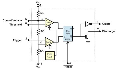
Then you will find a SR latch, and the output of comparators is the input of this latch. There is a PNP and NPN transistor configuration also one for the reset of this latch and other one is connected to the Discharge pin of the IC. The special thing about this IC is that it can generate very accurate time delays.
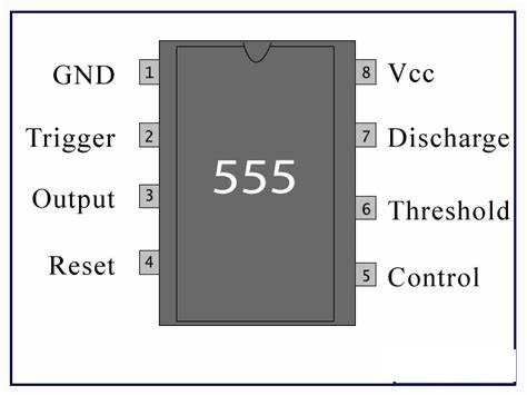
Pin diagram:
There are 8 pin in the DIP package of 555. It is made by Texas and nowadays manufactured in ST labs. These 8 pin of the IC are arranged as given in the Image.
For more package info download the original datasheet from here. Some more features are:
Output Can Source or Sink 200 mA
Output and Supply TTL Compatible
Direct Replacement for SE555/NE555
Normally On and Normally Off Output
Temperature Stability Better than 0.005% per °C
Astable configuration:
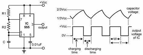
In the astable mode of this IC, the following circuit diagram is used. Capacitor is connected to 2,6 pin. Reset pin(4) is connected to VCC(8). Trigger(2) to Threshold(6) to make a loop or auto trigging circuit. Control voltage(5) is connected to ground with a bypass capacitor to avoid any noise. One resistor R1 is connected between pin 6 to 7 ( Threshold to discharge) and R2 is between 7 and 8(discharge and VCC). This configuration is only used for a stable mode to generate a specific frequency with fixed duty cycle. Let’s know what is happening inside to calculate duty cycle and frequency values.
Working of Astable mode:
When initially power is turned ON, Trigger Pin voltage is below Vcc/3, that makes the lower comparator output HIGH and SETS the flip flop and output of the 555 chip is HIGH.
This makes the transistor Q1 OFF, because Qbar, Q’=0 is directly applied to base of transistor. As the transistor is OFF, capacitor C1 starts charging and when it gets charged to a voltage above than Vcc/3, then Lower comparator output becomes LOW (Upper comparator is also at LOW) and Flip flop output remains the same as previous (555 output remains HIGH).
⦁ Now when capacitor charging gets to voltage above than 2/3Vcc, then the voltage of non-inverting end (Threshold PIN 6) becomes higher than the inverting end of the comparator. This makes Upper comparator output HIGH and RESETs the Flip flop, output of 555 chip becomes LOW.
⦁ As soon as the output of 555 get LOW means Q’=1, then transistor Q1 becomes ON and short the capacitor C1 to the Ground. So the capacitor C1 starts discharging to the ground through the Discharge PIN 7 and resistor R2.
⦁ As capacitor voltage get down below the 2/3 Vcc, upper comparator output becomes LOW, now SR Flip flop remains in the previous state as both the comparators are LOW.
⦁ While discharging, when capacitor voltage gets down below Vcc/3, this makes the Lower comparator output HIGH (upper comparator remain LOW) and Sets the flip flop again and 555 output becomes HIGH.
⦁ Transistor Q1 becomes OFF and again capacitor C1 starts charging.
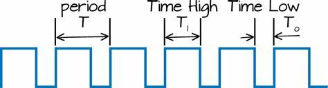
This charging and discharging of capacitor continues and a rectangular oscillating output wave for is generated. While capacitor is getting charge the output of 555 is HIGH, and while capacitor is getting discharge output will be LOW. So this is called Astable mode because none of the state is stable and 555 automatically interchange its state from HIGH to LOW and LOW to HIGH, so it is called Free running Multivibrator. Now the OUTPUT HIGH and OUTPUT LOW duration, is determined by the Resistors R1 & R2 and capacitor C1. This can be calculated using below formulas:
Time High (Seconds) T1 = 0.693 * (R1+R2) * C1
Time Low (Seconds) T2 = 0.693 * R2 * C1
Time Period T = Time High + Time Low = 0.693 * (R1+2*R2) * C1
Frequency f = 1/Time Period = 1/ 0.693 * (R1+2R2) * C1 = 1.44 / (R1+2R2) * C1
Duty Cycle: Duty cycle is the ratio of time for which the output is HIGH to the total time.
Duty cycle %: (Time HIGH/ Total time) * 100 = (T1/T) * 100 = (R1+R2)/ (R1+2*R2) *100
Here is the practical demonstration of the Astable mode of 555 timer IC, where we have connected a LED to the output of the 555 IC. In this 555 astable multivibrator circuit, LED will switch ON and OFF automatically with a particular duration. ON time, OFF time and Frequency can be calculated using above formulas.
Circuit diagram:
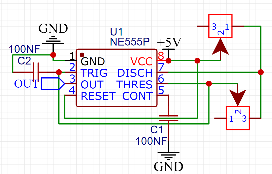
As you can see in the formulas given above the Frequency and duty cycle both can be adjusted using the values of R1, R2 and C1. In this case we are using fixed C1 and variable 100k resistors. First measure the capacitance according to the frequency and then you can trim the R1 and R2 accordingly. We are using 5 volt power supply with this circuit, but a 9v battery can also be used. In this arrangement of components only greater than 50% Duty cycle is possible for the lower duty new tutorial will be published soon.
Gerber files:
I made the PCB files according to the modified schematics, then exported them as Gerber files. If you want to use the same files then download them from here.
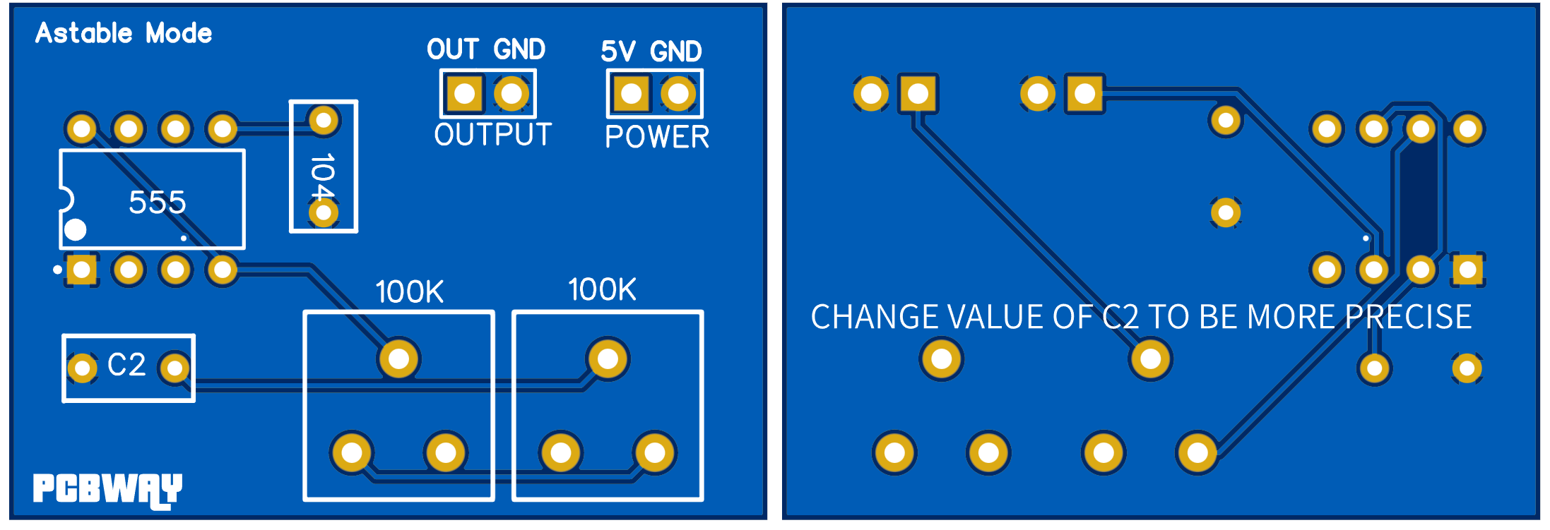
I am using PCBWAY prototype service for a long time, PCBWAY is China based PCB manufacturer deals in PCBA, SMT assembly, Stencil, Metal CNC, Flex PCB, 3-printing services and more. Sign-up to PCBWAY using this link and get free new user coupons.
Duty problem:
This configuration has a problem that even with a smallest resistance of zero the minimum duty cycle we can archive is 50%. To get more smaller values we have to do some modifications in the circuit. because making the resistor value even to zero ohms result in minimum duty cycle of 50%. Which will be explained in the next tutorial of 555.