h2w
h2w-
A minute of Fun
01/10/2023 at 13:58 • 0 commentsThe AI picture on the word "XiAleste" produce a cute miniature.
![]()
The AI's random art based on XiAleste PCB image.
![]()
-
The files now on the GitHub
01/08/2023 at 11:56 • 0 commentsThe PCB project files uploaded to github repository.
-
The voice board dimentions
01/07/2023 at 17:21 • 0 commentsThe voice board profile is about 35mm height.
![]()
-
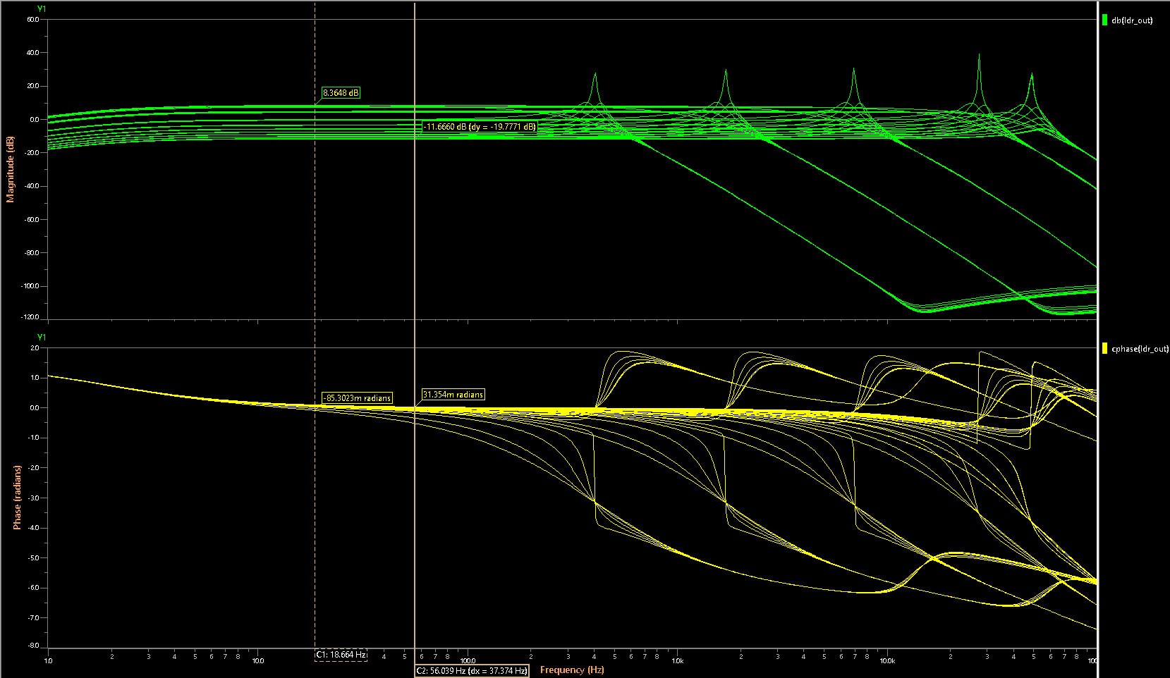
Steiner Parker Issue
01/07/2023 at 11:08 • 0 commentsFor some reason the Steiner Parker has different slopes. Left one is 12db/oct the right one is 6db/oct. Could be something wrong with my model.
![]()
-
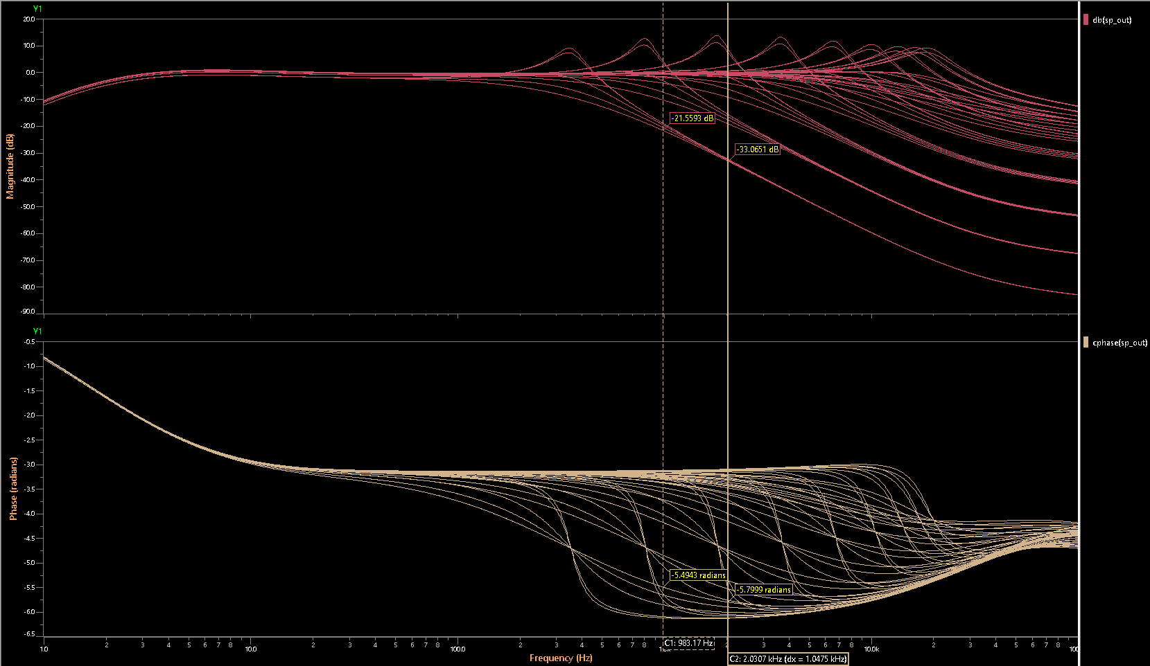
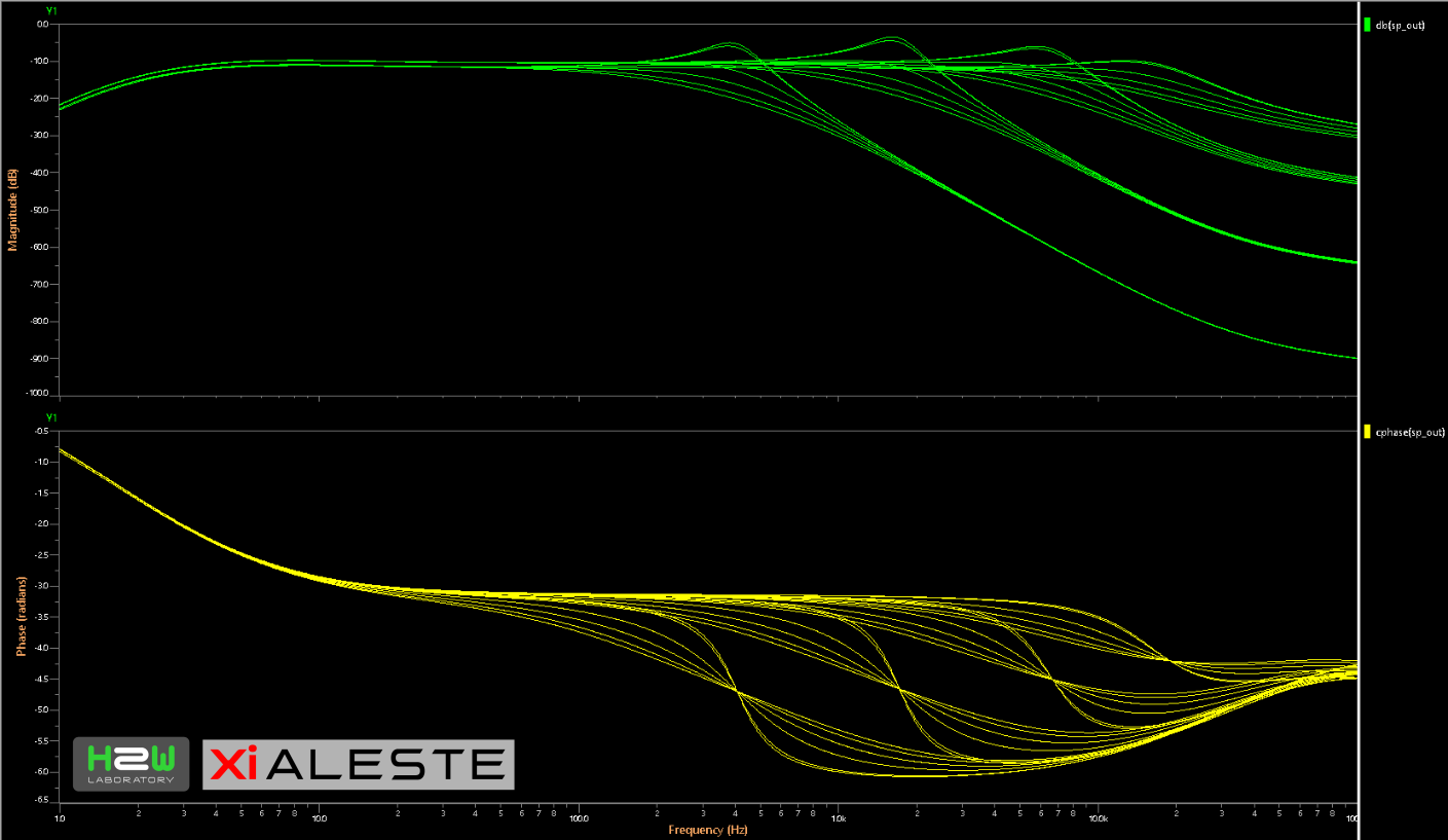
Steiner-Parker VCF
01/06/2023 at 18:42 • 0 commentsThis filter in my opinion makes the best result. With 12db per octave it makes very nice and predictable result (see image below). Love it! And the circuit is simple!
![]()
-
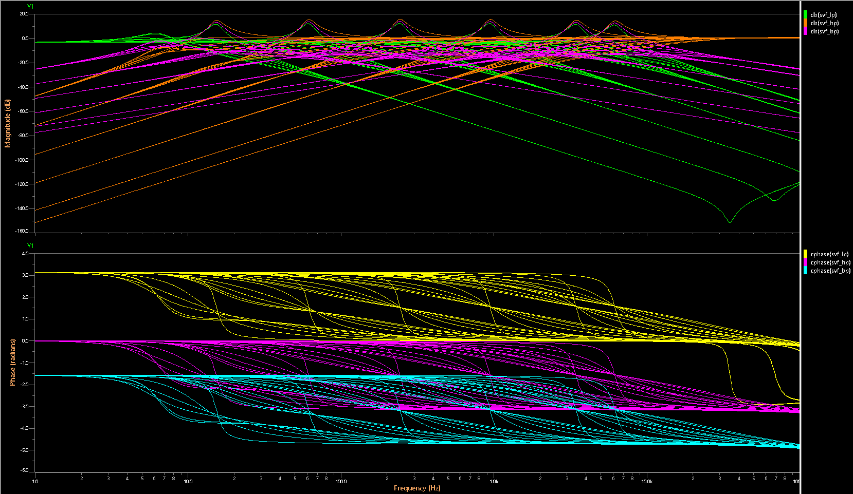
The State Variable Filter is good option
01/06/2023 at 14:36 • 0 commentsThis type of filter looks simple enough (so it match to XiAleste project) and very stable result. The image below has all filter modes LP,BP,HP. The coice board will mix those results in different proportions.
![]()
-
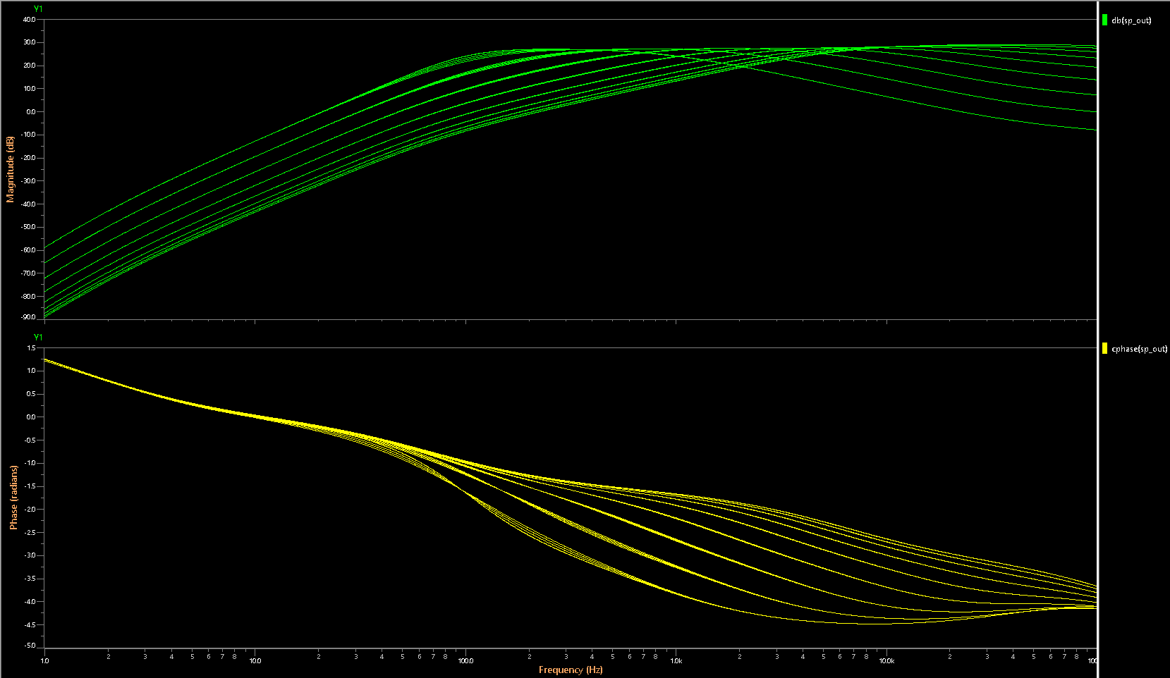
Why not Moog Ladder filter?
01/06/2023 at 14:22 • 0 commentsThe Ladder showed worst result compare with other filters.
BTW The way to analyze the Ladder and derivatives explained here https://www.timstinchcombe.co.uk/synth/Moog_ladder_tf.pdf
What I do not like most? There are several things:
1) Changing the output level with different resonance setting
2) The ladder requires precise parts and tuning.
3) The phase graph is extremely clucky. It could be something wrong with my circuit yet.![]()
-
The voice board design
01/06/2023 at 12:25 • 0 commentsAbout 3 weeks I have been working on a Voice board for this platform. The computer could produce sound w/o those boards, but with the boards the sound quality should go to semipro level.
I am doing this task now to confirm the voice board connector pinout before I will produce one unit.
The voice board is basically VCF. Each board has two of them. So as result 3 boards will have 6 separated channels. The board's output will goes to the mixer and also to the ADC for additional post processing (such as delay, chorus, reverb etc).
Currently I tried the next VCF circuits:
1 The state variable filter
2 Steiner Parker
3 Moog's ladderThe first two give a best result and I am deciding now -- should I put bought of them on the voice board. But in case if not, which one of them should I use.
![]()
-
PCB is almost ready for manufacturing
12/17/2022 at 16:34 • 0 comments![]()
The printed circuit board is ready. Now I need to think about what to do next with this project. So far no one has joined the project. It would be too presumptuous for me to continue on my own.
Anyway, I will post the source files on github shortly. -
FMC Bus - The Length Matching
12/17/2022 at 08:34 • 0 comments5mm Tolerance
![]()
XiAleste
XiAleste Next is an 8-bit home computer, which is compatible with software for the Amstrad CPC6128 released on 13 June 1985