 Ian Dunn
I've been a maker and an electronics enthusiast for my whole life. Designing custom PCB's is a specialty of mine. Somewhere along the way I realized that PCB's are a perfect medium for artistic works as well as electronic circuits. I have to give credit to Kelly Heaton for inspiring me to actually try it. I've created several circuit board art pieces and learned a lot along the way. I wrote this guide to share what I've learned about making art from printed circuit boards. I'll talk about making basic 2 dimensional PCB art, PCB art with electronic components, and how to make a PCB that is both beautiful and has electrical functionality. This guide is also relevant if your focus is PCB's that serve a primary function, but you also want them to look good.
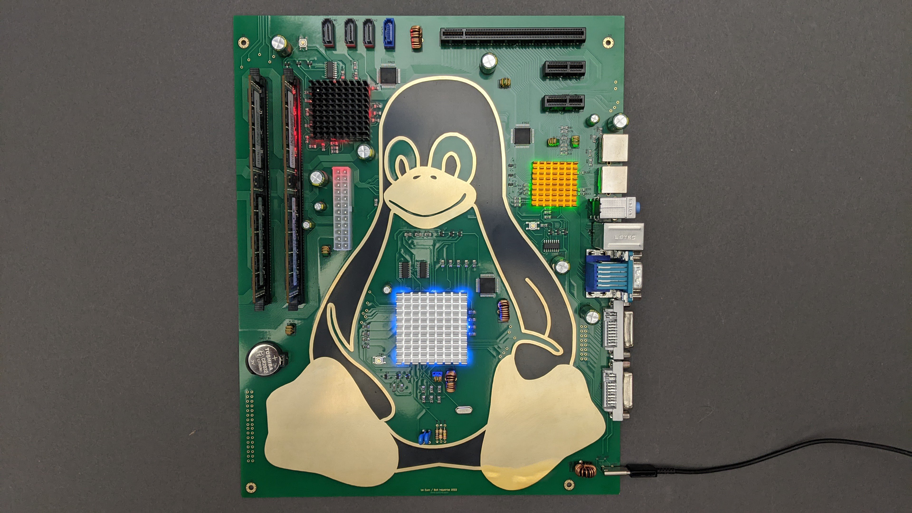
The Kickstarter campaign for the Tux Penguin ATX motherboard was unsuccessful. I had a lot of fun making it, and it will not be my last PCB art piece. Follow me here on Hackaday.io for more cool projects in the future. You can also visit my website, www.boltind.com where I have some PCB art for sale, and a lot of other cool open source stuff that's free for the taking.
It is a tradition of mine to write a Hackaday guide to accompany my Kickstarter projects, so here's everything you need to know to make your own circuit board art.
Solder Mask Colors and Copper Underneath
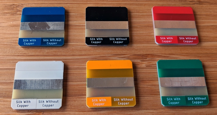
When it comes to PCB's, you're somewhat limited when it comes to colors. You can choose your solder mask color, and copper surface finish. Standard solder mask colors at most board houses are Green, Black, Red, White, Blue, yellow, and Purple. Black is the easiest to work with by far. It's usually a nice flat matte black color that looks really sharp. Some board houses seem to use a glossy black that is not nearly as nice. The other thing about black is that it['s opaque, so having copper underneath it won't really change it's appearance. All the same things are true about white. It is opaque, and white regardless of what is underneath it.
Pretty much any other solder mask color tends to be translucent, so you'll see the shiny copper traces or copper ground plane underneath it. This can be a problem with some colors. Green, Blue and Purple become washed out and dull if you add a copper ground plane underneath them. Smaller traces will be the same dull color, but it's not as noticeable on a small trace. It you want one of these colors, solder mask on top of the bare FR-4 without copper yields a much better color in most cases. The opposite is true of Yellow and red. I find that yellow looks a whole lot more Yellow with shiny copper underneath. Yellow on top of bare FR-4 is just plain ugly if you ask me. Red can go both ways. It's shiny and bright if placed on top of a copper ground plane. It's a little more muted if placed on top of bare FR-4, but still very red.
This is an image from an article on Hackaday.com that talks all about layers and solder mask colors. It does a great job of showing how each solder mask color looks. The link to the article is below.
Surface Finish
There are really only two options that I recommend for surface finish. ENIG (Electroless Nickel Emmersion Gold) or HASL (Hot Air Surface Leveling.) There are other options out there but they are a little exotic and a lot more expensive. I usually stick to ENIG. ENIG is a gold plated finish so it's more costly than HASL. HASL is just plain old silver colored solder in your choice of leaded or unleaded. There is not much of anything attractive about silvery gray solder, so ENIG is my go to choice. However I recommend always ordering the first board with HASL because no matter how confidant you are of your design, you will always want to change something when you actually get your board. Once you've got your board perfected with...
Read more »

 Josh Kittle
 Mike Teachman
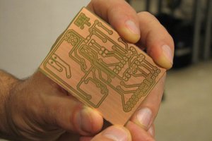
 PCB designer
 Michael Delaney
Good to see aesthetic pcbs discussed - this is needed, as most nerds have no sense of beauty, thus all the garish colors offered by board houses. As far as I am concerned, every board house should offer black FR4 with clear solder stop mask. Because I want to see all the pretty copper when I'm already paying for it, and the black FR4 is the perfect backdrop for it.