 agp.cooper
LogiSim Simulation
Nowadays I simulate my CPU designs with LogiSim. LogiSim is not without faults, but it is quite pleasing to see a simulation work, and reduces hardware debugging later.
Usually I try to be modular and use standard components, but ROM and RAM modules for LogiSim are built in. So I have to work with them.
Static AM Chips
My historical designs used LogiSim's "one asynchronous load/store port" RAM option as it can model typical Static RAM. I have tried to get the 7489/74189/74289 16x4b RAM chips, but each time I get fake chips. I cannot get 2112 SRAM chips anymore, and the ones I had are used up. I did use a CMOS 6116 (2kx8b) SRAM for the CHUMP V5, but this chip is overkill for this project.
I bought some PCD5101p dual port 256x4b CMOS SRAM chips, which seem plentiful on the Internet, so that is what I will be using. It is possible to design a CPU in this series that could access 256 nibbles of RAM. These chips however, require the LogiSim "separate load and store ports" RAM option.
Using a dual port SRAM saves a tristate buffer in the ALU module.
PROM
In previous designs, I used the AT26C256 Flash PROM. It is nice to use if you have a programmer. Using a diode DIL switch PROM instead adds a "home built" and "hands on" charm to the project.
If only I could do the same for the RAM!
16 Bit Address Space
Using a diode DIL switch PROM caps the address space to 16 bit. It is just a practical limitation due to the component count.
LogiSim Design
I am up to version 3 here:

Reset/Clock/Run/Stop/Step
Here is the CPU control circuit:
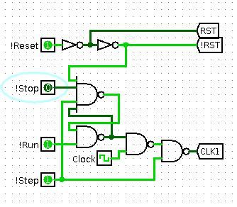
This circuit provided Reset, Run, Stop, and Single Step. In my mind it is a work of art!
Here is the actual schematic:

The schematic considers switch debounce and the two phase clock.
The ALU
Previously I used the 74LS181 ALU:

The ALU was reworked to use discrete chips:

Version 3 is based on dual port static RAM (i.e. separate inputs and outputs), in this case the tristate buffer is not required:

But I want to change the ADD instruction to ADC (add with carry). This requires the a clocked D-Latch (i.e 74HC74) between Cout and Cin of the 74HC283.
I am also considering the replacement of JNC (jump on not carry) with JNZ (jump on not zero).
Control Logic
The control logic is somewhat simpler now:
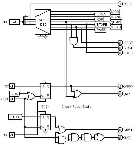
Note: !PAGE is not used and has been relabelled !SPARE on the main page.
I am thinking of using !SPARE to prefix an alternate set of instructions, but not until later in this series of CPUs.
AlanX
Discussions
Become a Hackaday.io Member
Create an account to leave a comment. Already have an account? Log In.