 Bharbour
I have been working out a style for drawing top level schematics with a PCB schematic capture package. After a fair amount of messing around, this is the resulting drawing of my Timeserver project.
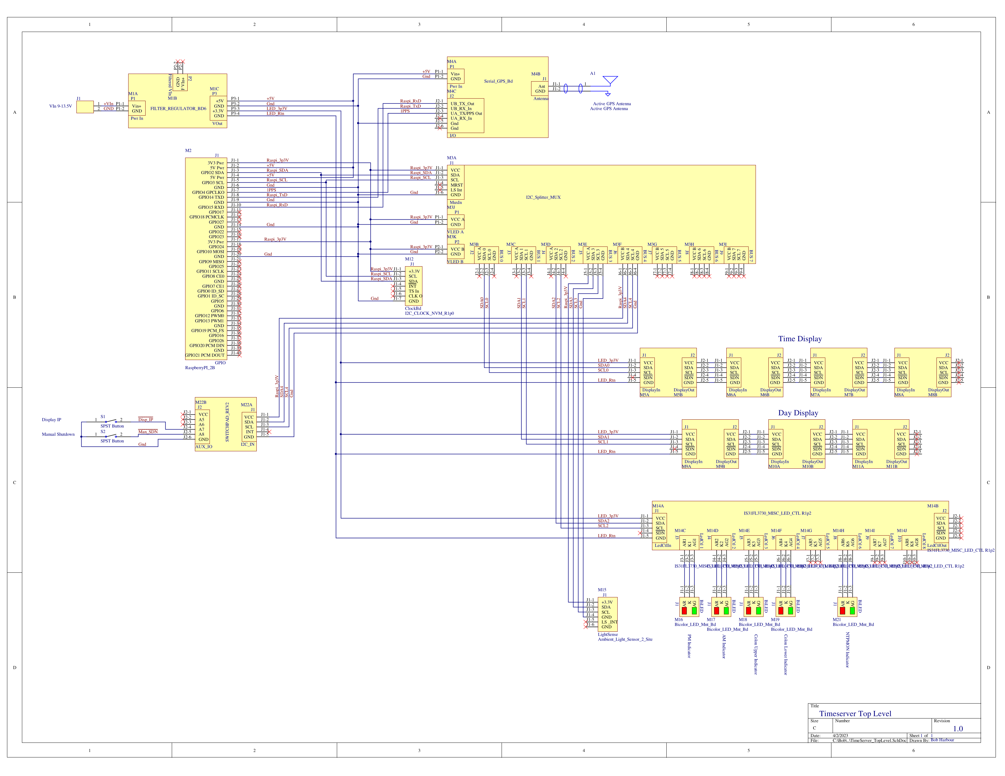
Some things could use a little more work, but as a document, this works for me.
Each individual board is created as a component in my CAD system. Connectors on the board are implemented as "parts" in the same way that you would have two (or 3 if you separate power supply pins) "parts" in a dual OPAMP component. This allows flexibility in how you place the individual connectors on a drawing. The one thing it does not allow is compiling into a net list. Each connector has pins "1", "2", "3"... and this confuses my CAD system because it would not make sense for a dual OPAMP to use pin 1 in both "parts" (other than the power supply pins). The way around this would be to include the connector ID in the pin number. For example on connector J1, pin 1, a name of J1-1 would be a unique name and the CAD system would be fine with that. The down side of this method is that the pin numbers become long and take more space on the drawing.
The connectors are placed on the drawing and I have drawn a rectangle around each one to represent a board. It would not have to be done this way, it would be possible to scatter the connectors around the schematic in the same way that groups of signals are handled on schematics with large, complex IC's on them. I tend to like working with the connectors for a board gathered into one spot because it makes it easier when poking around with a scope probe to find the signal you are looking for. There is definitely a limit to how far this approach can be scaled though.
Wire colors would be nice too. I think I can attach colors as a property to wires, but I have not gotten that far yet.
I went back and edited the schematic library and the top level schematic. The end result is fine, and now it compiles to produce a net list. Top level schematics tend to be large drawings anyway, so the change is not a problem. Being that the purpose of this is to establish the method and start building a library of the PCBs that I have designed, I want to get the best result that I can.
Has anybody else got a method for drawing top level system schematics and wiring harnesses that works?
Discussions
Become a Hackaday.io Member
Create an account to leave a comment. Already have an account? Log In.