 DIY GUY Chris
roblems & Objectives
A lot of Dev Boards like Arduino, STM, ChipKit etc (Even micro computers like Raspberry Pi) has a limited number of Digital input and output pins, which is a serious problem for the makers while creating them projects, especially when the Dev Board should be connected to an important number of peripheric (Exemple: the 5x5x5 LED Cube where you need to control more than 100 LED). Our goal is to satisfy the users desires by making a Hardware and Software solution to add more Digital I/O pins to your Dev Boards.
The solution
The IOExtension module is based on four shift registers (74HC595) to provide 16 Digital Inputs and 16 Digital Outputs, you will need only four pins in your Dev Board to control the module, plus the Vcc and the Gnd pins.
The use of this module is so handy because the MEGA DAS community developed an Arduino software library to grant you using the module with a minimum code instructions.
About the main component (74HC595)
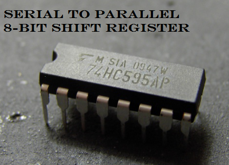
The Hardware part is so simple and based on the 74HC595 shift register, it is an easy and inexpensive way to increase the number of digital I/O pins on your Dev board. This integrated circuit is inherently digital, like the digital pins on the Arduino it means that they can only read or write HIGH or LOW logic levels, they should not be used to read data from analog sensors or potentiometers.
We can find a lot of hardware and circuits based on this kind of shift registers like theAdafruit motor shield, 7 segment module. The use of this circuit is so handy and a great hands-on approach of the multiplexing an efficient technique for controlling many components wired together.
you can order 5 pics of 74HC595 online for less than 6$ Amazon order link.So how to use the 74HC595!!
The circuit provides three interfacing pins which are the SHIFT_CLOCK (SH_CP), the LATCH_CLOCK (ST_CP) and the Data pin (DS).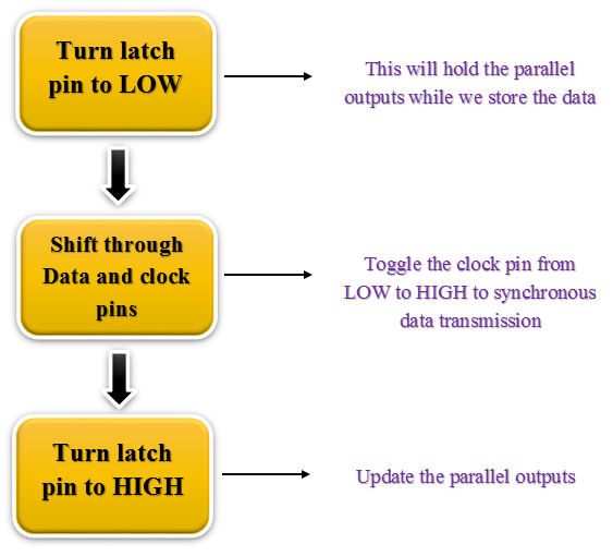
The first step consist on storing the data in the storage register and to do so we need set latch pin to LOW to disable the outputs, this way the output pins won't change as we are sending in new data to the 74HC595.
The next step is sending the data bit by bit serially, by pulsing the clock pin and sending each byte of new data out the data pin.
The last step is setting the latch pin high. This way the register will update the (parallel outputs).
You can find more details about this integrated circuit in its Datasheet.
I’m just explaining how the shift register operates but, we’ll not do all this work because we gonna use the Arduino SPI library to control the whole thing and don’t forget that you will have a library to control the module, just a last information about the shift register it has 8 parallel outputs (Q0-Q7) and one serial output (Q7') for cascading.
The Hardware design (The circuit)
The IOExtension module is based on four shift registers (74HC595) to provide 16 Digital Inputs and 16 Digital Outputs, you will need only four pins in your Dev Board to control the module, plus the Vcc and the Gnd pins.
In order to have 32 I/O pins we will use four shift registers (74HC595) as showed in the schematic. The four registers should have a synchronised Data and update the all outputs and the inputs at the same time, this is why we should connect all the LATCH_CLOCK pins together and all the SHIFT_CLOCK too, but the Data pin of your first register will be connected to you Arduino board and the rest of registers will be connected to each other through the serial output (Q7') that means connect the serial output of your first shift register to the data pin of the next shift register and so.
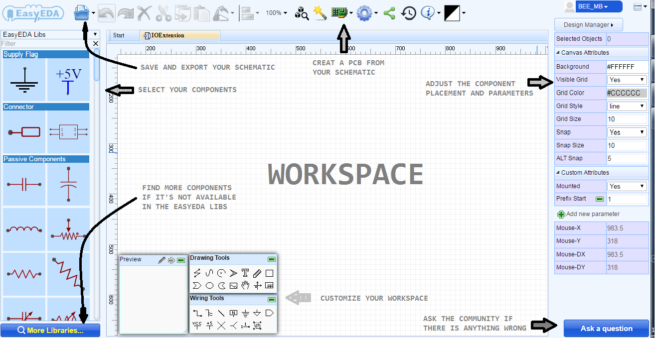
I highly recommend the easyEDA website to make your PCB.
BUT What is the easyEDA!It's a free online Electronic design automation community that allows the creation, testing and editing of schematics and PCBs.
Find the link to the easyEDA platform here.
This online program is supported in all platforms even android, with easyEDA you can make a Schematic Capture for your documents, Circuit Simulation, Online PCB Designing...
Read more »
 George Albercook
 Sagar 001
 Nigel
Nigel