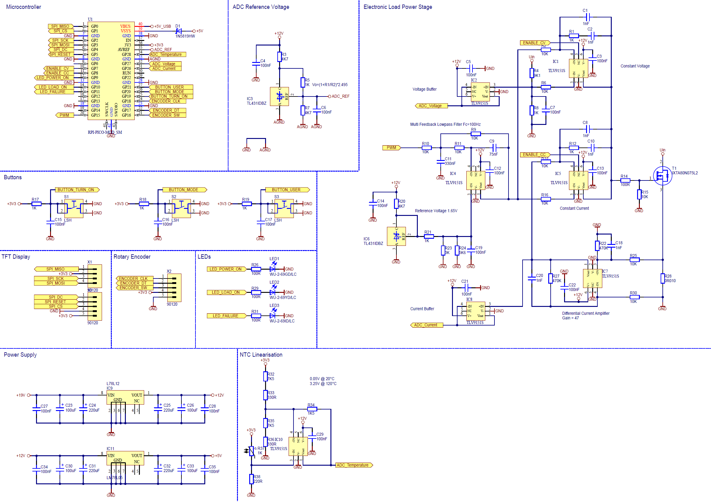
• A rough description

    Per-Simon Saal06/17/2023 at 14:09 0 comments

    I started with the idea to develop an electronic load because I wanted to learn something about OP AMPs and the linear operation mode of MOSFETs. After some research and simulating a lot I finished the schematic. But it is not finished yet.

    The main part on the right shows the power stage. There are several OpAmps.

    First, the differential amplifier amplifing the voltage difference over the shunt resistor.

    Second, the constant current error amplfier driving the MOSFET gate to achive the desired current at the shunt.

    Next the constant voltage error amplifier reading the voltage over the MOSFET and the shunt. Also feeding the gate in parallel with the CC OpAmp.

    Two buffers provide the controller with the current and voltage of the load.

    A multi feedback inverting low pass provides the reference voltage for both error amplifiers. The lack of an DAC at the RP2040 results in low passing a PWM signal. This low pass has very little ripple. But is a bit slower. This is not a bug but a feature. More on this later.

    The low pass needs a precise reference voltage. This is generated with the TL431.

    A NTC measures the temperature close to the MOSFET. The circuit arount it generates a linear voltage for the controller to read. It is designed to read temperatures from 20°C to 100°C.

    Some buttons and LEDs are never wrong and will find a good function.

    The power supply is completely linear to provide a smooth voltage for the OpAmps.

    More details on the function will follow.