In the last post, I mentioned how the MOSFET in the load stage, which is supposed to turn on and off the load resistor, was oscillating. I've been looking in to this more and I think I understand what I did to create the issue, even if I don't fully understand exactly how the oscillator I managed to create works.
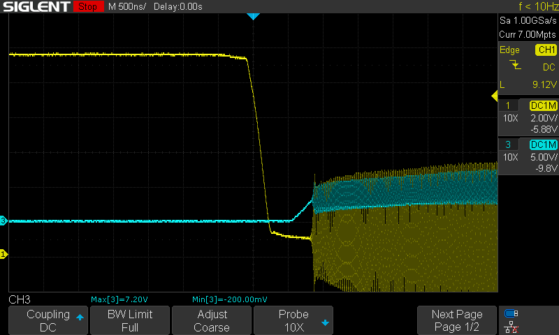
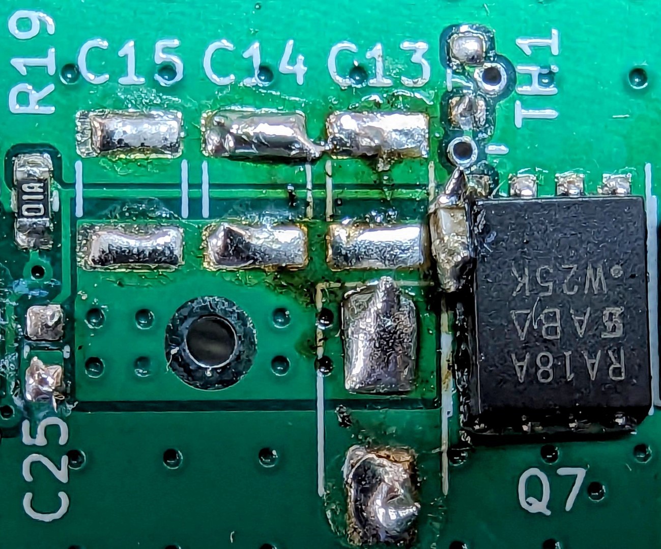
I present to you, our culprit:
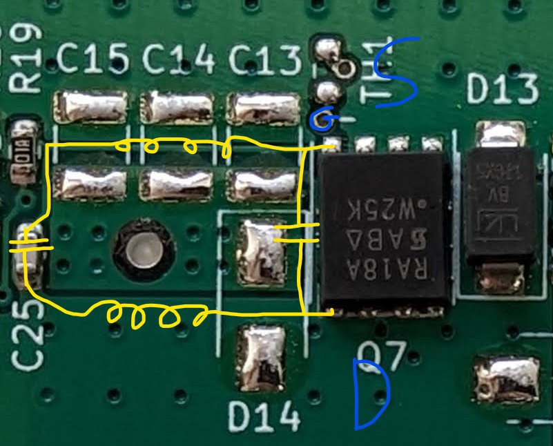
Do you see it? While it might look like an innocent trace, it is really an inductor in disguise.
I believe the capacitor I added, Cgd (C25), the gate-drain capacitance inside the MOSFET, the parasitic inductance of the traces, and the amplification of the MOSFET, have formed an oscillator.
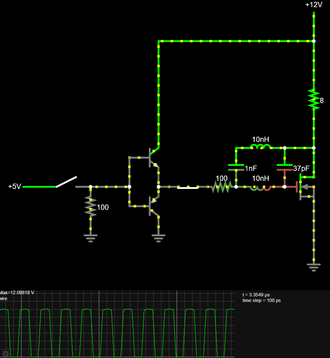
If you run the numbers, 1nF cap + 12nH inductance (ballpark guess) resonates at 46MHz, which is at least in the same order of magnitude as the 72MHz I'm measuring.
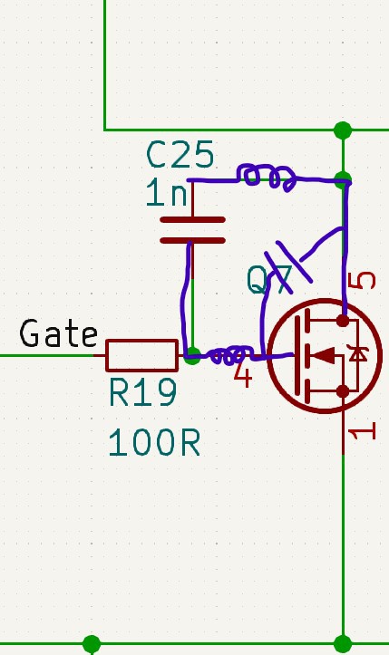
The gate-drain cap was added in the first place to slow down the MOSFETs turn-off transition. This lowers the slew rate of the drain-source voltage, which slows down how quickly current must stop flowing through the inductance of the cables and load resistor (dI/dt), which thus reduces the inductive voltage spike across the MOSFET. However, in exchange more power is dissipated in the MOSFETs when switching. This cap, combined with the other mitigation strategies I'll describe in the future (RC snubber, TVS diodes, flyback diodes), should be enough to manage the inductive spikes for the 8R to 0.5R load stages (Currents 1.5-24A). The 0.1R load stage that will operate at 120A needs something a bit more special.
To test this and remove nearly all of the trace parasitic inductance, I managed to cram the gate-drain capacitor right next to the MOSFET and solder it in. One end of the capacitor is actually soldered to the small bit of exposed drain terminal that sticks out the side of the MOSFET package.
I don't think it's possible to get any lower inductance than this. The reason I didn't do this during the PCB layout is that I prioritized the trace inductance from the MOSFET to its TVS, and to the large capacitors used in the inductive energy capture circuit for the 0.1R load stage variant.
The result is very good:
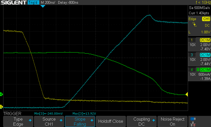
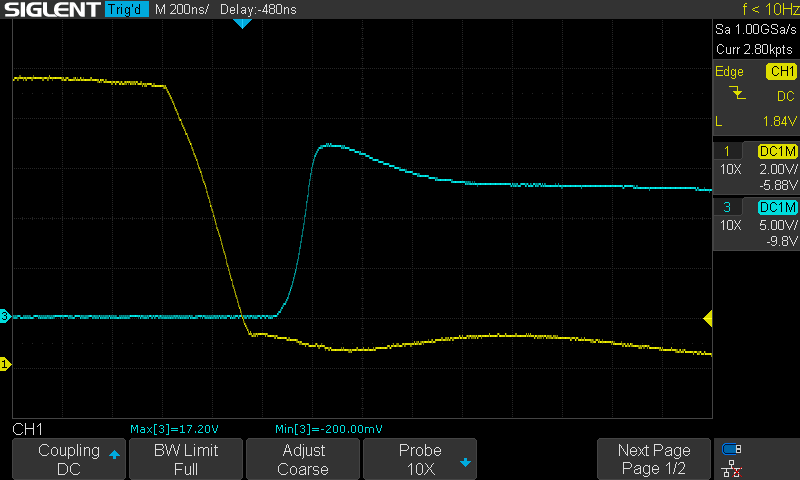
For comparison, here is the turn-off waveform with no gate-drain capacitor:
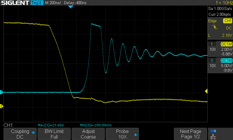
Just for fun, here is the waveform with no RC snubber. I believe the ringing is the inductance of the cables (700nH-ish?), the C_oss capacitance of the MOSFET (264pF), and the capacitance of the TVS (900pF). It rings at 6 MHz which is quite close to the 5.6 MHz I calculate for those values. :
Although it feels less elegant, I'm probably going to leave the gate-drain capacitor off of the next load stages I assemble, and I'll try increasing the gate resistor to 3.3k to slow down the transition speed instead. Simulation shows that should work about the same. On a future revision of the load stage PCB, I'll add a footprint to put a gate-drain cap right next to the FET.
Next up: why is there such a long 30us delay between the FET_EN logic signal going low, and the gate drive circuit output going low? I'm kind of regretting doing the gate driver in discrete components at this point.
Discussions
Become a Hackaday.io Member
Create an account to leave a comment. Already have an account? Log In.