Let’s take a look at that turn-off delay issue.

If my goal is to be able to do 100us pulses, having a 30us turn-off delay is a problem. The timing is fairly critical because I need all of the load stages to switch at the same time, more or less. I’d also like the option to precisely sequence the load stages to either control the DUT current slew rate, or to compensate for the higher inductance load resistors which have a slower current slew rate by turning on some of the “faster” low inductance stages briefly. I think I’d like the load stages to respond within 5us, and ideally faster.
After more learning and research, I think I’ve determined the root cause. In short, I picked a cheap and slow optocoupler with phototransistor output, the slow kind. (PN: LTV-816S)
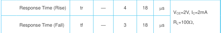
I didn’t read the datasheet closely enough and was relying on the listed 3-4us response time, but I didn’t pay attention to the test conditions. They actually specify that response time with a V_ce of 2V, an R_load of 100R, and I_c of 2mA, which actually means they are measuring a voltage swing of 200mV around a 2V signal. Definitely not the 0-600mV swing needed in my design to switch the following BJT inverter. Also, I was using an output pull-up of 3.3k which made things much worse.


I recreated the optocoupler and inverter section of the gate drive circuitry on a breadboard and used that to confirm the issue. Although, I could pretty clearly see how long it was taking the optocoupler output to rise measuring in-circuit on the load stage.


I also tried to reproduce the datasheet specs under their test conditions, with 2.2V Vcc on the optocoupler output, a 100R pullup resistor, and then reducing the input drive current until the voltage when low was 2V, thus a 200mV swing or 2mA I_c. I was able to get 8.3us response time on input going low (Tr), and 14.5us response time on input going high (Tf). Technically within the max specifications I suppose but not good enough for me.
I found reducing the input drive current would reduce the turn-off delay, but it would also increase the turn-on delay so it’s not much of an improvement. Also, reducing the designed input drive current to keep the phototransistor from saturating would mean we are depending on the optocoupler CTR to stay the same, and that spec can vary wildly between parts and over temperature, I believe.

I also didn’t want to reduce the value of the optocoupler output pullup resistor, because that resistor is always drawing current from the DUT, and so it directly affects the quiescent current of the load stage. This means even at 3.3k, assuming a DUT voltage of 12V, the load stage has a quiescent current of 3.6mA. With 53 load stages, that becomes 191mA drawn from the DUT even when all the load stages are off. That’s a lot more than I’d like on principle alone, even if it wouldn’t matter much in my application. This ties in with the question of “Why power the gate drivers from the DUT anyways?” which I need to address in the main project details section at some point.
Knowing that my optocoupler circuit is fundamentally flawed, that left a few solutions:
- Do nothing in hardware and compensate for the turn-off delay in software
- In theory this could work, however the delay also varies with the DUT supply voltage. It also varies non-linearly, where it might be 30.7us at 3.3V, 28.8us at 6V, and then 30.4us at 12.2V. It might be possible to model the change in delay vs input voltage to adjust the compensation dynamically. Or I could even implement a calibration routine to measure the delay time of each stage from the FET_EN signal to a rise measured on the current sense signal. The current sense amplifier signal bandwidth is low but we’d only care about delay time, not necessarily rise time, so I think it might be possible to use that to measure delay. This is a lot of complexity, all to work around a fundamental hardware issue though.
- Use the same optocoupler with a more complex circuit that lets the optocoupler stay out of saturation and keeps the voltage swing on the optocoupler collector minimal to reduce the effect of the B-C miller capacitance, and thus reduce rise and fall times.
- This adds more transistors, takes more time, and adds more complexity. All just to try to avoid paying a little more for the next solution.
- Performance still might not be great.
- Use a better photodiode-based optocoupler like a 6N136, with a similar circuit to what we already have
- This adds some cost for the better part. $0.348 for a 6N136S vs $0.145 for the currently used LTV-816S (Digikey pricing at 100 qty)
- The 6N136 has more strict absolute max ratings, particularly a 15V max VCC voltage on the output side which will be a problem. It also requires more input drive current and possibly a capacitor decoupling capacitor. Any capacitance on the load stage concerns me because with the cable inductance it directly causes current to be injected into the DUT when the load stage is turned off.
- The datasheet promises much faster response times of 1.5us maximum even at higher output pullup resistor values.
I settled on the last option: redesign the gate drive circuitry to use a better optocoupler, the 6N136.
In the next post I’ll go over the new design with the 6N136, the extra protection circuitry it requires, and its performance.
Discussions
Become a Hackaday.io Member
Create an account to leave a comment. Already have an account? Log In.